
The Limits of Scaling and the Rise of Materials Science
For decades, the semiconductor industry has relied on Moore's Law – the observation that the number of transistors on a microchip doubles approximately every two years – to drive progress. This relentless pursuit of smaller transistors, achieved through advances in lithography and process technology, has fueled the exponential growth in computing power we've come to expect. However, as we approach the fundamental physical limits of silicon and the astronomical costs associated with ever-finer lithographic nodes, the industry is increasingly looking beyond traditional scaling for its next leap forward. This shift places materials innovation at the forefront, transforming how chips are designed, developed, and manufactured.
The challenge is no longer just about shrinking features; it's about finding new materials that can enable novel device architectures, improve performance, reduce power consumption, and even offer entirely new functionalities. This requires a deeper integration of materials science expertise much earlier in the design and development cycle. The traditional model, where materials were often considered late in the process, is giving way to a more collaborative, co-development approach. This means material scientists, device engineers, and process engineers are working hand-in-hand from the conceptualization phase, a paradigm shift that accelerates the journey from laboratory discovery to high-volume manufacturing (fab).
New Materials for New Architectures
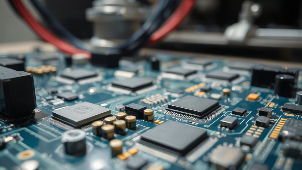
The limitations of silicon as a sole workhorse are becoming apparent. While it has served the industry admirably, new materials are essential for overcoming inherent constraints. For instance, the drive for lower power consumption in mobile devices and high-performance computing necessitates materials with superior charge carrier mobility or different bandgaps. This has led to significant research into materials like Gallium Nitride (GaN) and Silicon Carbide (SiC) for power electronics, offering higher efficiency and operating temperatures than silicon. Beyond power, in logic and memory, researchers are exploring 2D materials such as graphene and transition metal dichalcogenides (TMDs) for their unique electronic properties, potentially enabling transistors that are smaller, faster, and more energy-efficient than current silicon-based technologies.
Furthermore, the integration of heterogeneous components onto a single chip – known as chiplets or 3D integration – presents another fertile ground for materials innovation. Advanced packaging techniques require new materials for interconnections, thermal management, and structural integrity. For example, novel dielectric materials with lower dielectric constants (low-k) are crucial for reducing signal delay and crosstalk in densely packed integrated circuits. Similarly, advanced thermal interface materials (TIMs) are vital for dissipating heat generated by increasingly powerful and compact chip designs, preventing performance degradation and ensuring reliability. The development of new bonding materials, underfills, and encapsulants that can withstand extreme operating conditions and ensure long-term reliability is paramount for the success of these advanced packaging strategies.
Co-Development: From Lab to Fab at Speed
The path from a promising new material discovered in a research lab to its widespread adoption in a high-volume semiconductor fab is notoriously long and complex. Historically, materials were often developed in academic or research settings, with the onus on chip manufacturers to figure out how to integrate them into their existing processes. This sequential approach is too slow for today's rapidly evolving technological landscape. The modern imperative is for deep co-development, where materials suppliers, equipment manufacturers, and chip designers collaborate closely from the outset.
This collaborative model allows for a more holistic approach to problem-solving. Material scientists can tailor material properties not just for intrinsic performance but also for compatibility with existing or future manufacturing equipment and processes. Device engineers can provide crucial feedback on how material variations impact device performance and yield. Process engineers can identify potential manufacturing challenges and work with equipment vendors to develop the necessary tools for deposition, etching, and metrology. This iterative feedback loop, where insights from one stage directly inform the next, significantly shortens development cycles and reduces the risk of costly integration failures. It's akin to a chef and a farmer working together from the seed to the final dish, ensuring the ingredients are perfect for the intended culinary creation.
The Economic and Strategic Imperative
The growing reliance on materials innovation is not merely a technical evolution; it carries significant economic and strategic implications. For materials suppliers, it represents a substantial market opportunity. Companies that can develop and reliably supply novel, high-performance materials for next-generation chips stand to gain a significant competitive advantage. This also drives investment in advanced manufacturing capabilities and R&D within the materials sector itself.
For chip manufacturers, mastering materials innovation is becoming a key differentiator. It allows them to create products with unique performance characteristics that are difficult for competitors to replicate through process scaling alone. This can lead to higher margins, entry into new markets, and a stronger intellectual property portfolio. Governments are also recognizing the strategic importance of materials innovation, with increased funding and policy initiatives aimed at securing domestic supply chains for critical materials and fostering innovation in semiconductor manufacturing. The ability to control and innovate at the materials level is becoming as crucial as mastering lithography for national technological sovereignty and economic competitiveness.
Looking Ahead: Integration and Sustainability
The future of semiconductor manufacturing will undoubtedly be shaped by continued advancements in materials science. We can expect to see an even greater diversity of materials being integrated into chips, including novel semiconductors, advanced dielectrics, and specialized metallization. The focus will not only be on performance but also on sustainability. Developing materials and processes that are more energy-efficient, use fewer hazardous chemicals, and generate less waste will become increasingly important, driven by both regulatory pressures and market demand.
The challenges are substantial, requiring significant investment in R&D, advanced metrology, and sophisticated process control. However, the potential rewards – chips that are faster, more power-efficient, and capable of entirely new applications – are immense. As the industry moves beyond the traditional playbook of scaling, materials innovation is emerging as the primary engine for future progress, ushering in a new era of semiconductor design and manufacturing.