The HBM Bottleneck for Edge AI
High Bandwidth Memory (HBM) has become the de facto standard for AI acceleration, particularly in data centers and high-performance computing. Its stacked DRAM architecture, coupled with a wide interface, delivers the massive throughput required for training large language models and complex AI workloads. However, for AI inference at the edge – the processing of AI models on devices closer to the data source, such as smartphones, autonomous vehicles, and IoT devices – HBM presents significant challenges. These include high power consumption, substantial cost, and a form factor that is often too large for space-constrained edge devices.
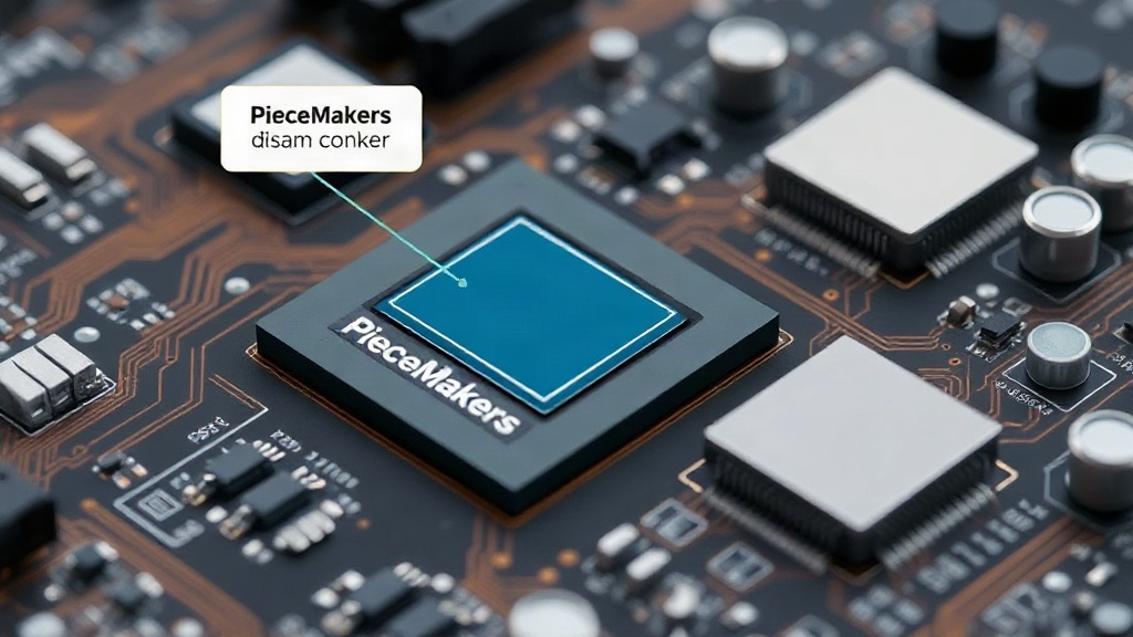
PieceMakers, a DRAM designer backed by Nanya Technology, is betting that the future of AI inference memory will diverge from this reliance on HBM. The company’s strategy centers on a novel architectural approach that fuses DRAM stacks directly to the processor using advanced hybrid bonding techniques. This method aims to provide a more efficient, cost-effective, and power-optimized solution specifically tailored for the demands of edge AI inference.
The fundamental premise behind PieceMakers' innovation is to address the specific memory bandwidth and latency requirements of inference tasks, which differ from the massive, sustained throughput demands of training. Inference often involves processing smaller batches of data more frequently, requiring rapid access to model parameters and intermediate computations. While HBM excels at raw bandwidth, its overhead in terms of power and complexity makes it suboptimal for many edge applications where energy efficiency and cost are paramount.
Hybrid Bonding: The Key Enabler
The cornerstone of PieceMakers' approach is the application of hybrid bonding technology. Traditionally, DRAM chips are packaged separately from processors and connected via a printed circuit board (PCB) or interposer. This introduces signal integrity challenges and limits the density and bandwidth achievable. Hybrid bonding, a technique more commonly seen in advanced packaging for high-end GPUs and CPUs, allows for direct, face-to-face connection of dies with extremely fine-pitch copper-to-copper interconnects.
By fusing the DRAM stack directly to the processor die using hybrid bonding, PieceMakers can drastically shorten the physical distance data must travel. This reduction in interconnect length leads to several critical advantages:
- Reduced Latency: Shorter signal paths mean faster data transfer, crucial for real-time AI inference applications that demand immediate responses.
- Increased Bandwidth Density: Hybrid bonding enables a much higher density of interconnects compared to traditional wire bonding or flip-chip methods. This allows for more data pathways between the processor and memory, effectively increasing the usable bandwidth without the extreme width of HBM interfaces.
- Lower Power Consumption: Shorter, more efficient electrical connections require less power to drive signals, a significant advantage for battery-powered edge devices.
- Smaller Form Factor: Eliminating the need for separate HBM stacks and their associated packaging components allows for more compact System-in-Package (SiP) solutions, enabling smaller and lighter end products.
This technology is not entirely new in concept, but PieceMakers’ focus is on applying it specifically and cost-effectively to the memory needs of edge AI. They are leveraging Nanya Technology’s expertise in DRAM manufacturing to optimize the DRAM stacks for this integration. The challenge lies in integrating the complex process flows of logic (processor) and memory (DRAM) manufacturing while maintaining yield and cost targets suitable for mass-market edge devices.
Diverging from HBM: A Strategic Bet
PieceMakers' decision to bet against HBM for edge AI is a bold one, given HBM’s established position. HBM, particularly HBM3 and its successors, offers unparalleled bandwidth and capacity, making it the go-to for data center AI training and inference. However, its cost, power draw, and physical footprint are prohibitive for many edge scenarios. For instance, a smartphone or a smart camera simply cannot accommodate the complex thermal and electrical requirements of an HBM stack.
The company’s strategy recognizes that inference workloads, while computationally intensive, have different memory access patterns than training. Inference often involves loading a model and then performing many forward passes, each requiring rapid access to specific parameters. This pattern can be satisfied by a memory solution that offers low latency and sufficient bandwidth density, even if it doesn't match the peak theoretical bandwidth of HBM. PieceMakers’ direct-bonded DRAM aims to hit this sweet spot, providing a performance uplift over traditional DDR memory while remaining more power-efficient and cost-effective than HBM.
The implications for the edge AI market are substantial. If PieceMakers can successfully commercialize this technology, it could unlock new levels of performance and capability for on-device AI. This would enable more sophisticated AI features to run locally, reducing reliance on cloud connectivity, enhancing privacy, and improving responsiveness. Think of advanced on-device natural language processing, real-time object recognition with greater accuracy, or complex sensor fusion for autonomous systems – all running efficiently on compact, power-constrained hardware.
The Market Landscape and Future Outlook
The semiconductor industry is in a race to provide optimized solutions for the rapidly expanding edge AI market. While HBM dominates the high-end, there is a clear need for specialized memory architectures at lower power and cost points. Companies are exploring various approaches, including advanced DDR variants, specialized SRAM configurations, and novel non-volatile memory technologies. PieceMakers’ direct-bonded DRAM represents a significant contender in this space, leveraging established DRAM manufacturing processes with cutting-edge packaging technology.
The company began trading in Taipei on September 16th, signaling its readiness to move from design and development into broader market engagement. This public offering will likely provide the capital needed to scale production and forge partnerships with chip manufacturers and device makers. The success of PieceMakers hinges on its ability to demonstrate not only the technical superiority of its solution but also its economic viability and manufacturability at scale. If they can achieve this, they might just redefine what’s possible for AI processing on the edge, proving that specialized memory solutions can indeed diverge from the HBM paradigm.
What remains to be seen is how quickly and broadly this technology can be adopted. The integration of hybrid bonding into mass-produced edge AI chips requires close collaboration between logic designers, memory manufacturers, and advanced packaging foundries. The ecosystem needs to mature to support these highly integrated solutions. PieceMakers’ challenge is to build that ecosystem and convince the market that their vision of a HBM-less edge AI future is not only technically feasible but also the most practical path forward.