Advanced Lithography Demands Predictive Simulation
The relentless drive for smaller, faster, and more power-efficient chips hinges on mastering advanced lithography techniques. As feature sizes shrink and complexity increases, particularly with the advent of high Numerical Aperture (NA) Extreme Ultraviolet (EUV) lithography, traditional methods of predicting silicon behavior are becoming insufficient. Engineers are now turning to sophisticated optical simulation tools to forecast how new chip designs will perform years before the first test wafers can be manufactured and analyzed. This shift is critical for mitigating risks, optimizing designs, and accelerating the development cycle in a highly competitive semiconductor industry.
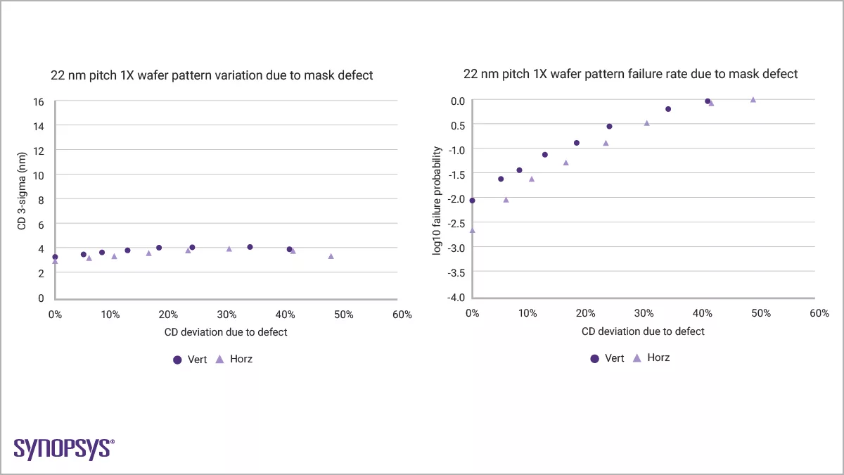
High-NA EUV lithography, a key enabler for sub-2nm process nodes, introduces unprecedented challenges. The physics of light interaction with mask patterns and wafer materials at these scales are incredibly complex. Small variations in mask design, illumination conditions, or resist properties can lead to significant deviations in the final patterned features on the silicon. These deviations, often manifesting as critical dimension (CD) variations, pattern placement errors, or stochastic defects, can render entire chip designs unusable or severely compromise performance. The cost and time associated with fabricating and testing physical wafers mean that identifying and correcting such issues early in the design phase is paramount.
Traditionally, the semiconductor industry relied heavily on experimental data from test wafers to validate simulation models and identify fabrication issues. However, for cutting-edge nodes, the lead time for developing new lithography equipment, masks, and materials extends for years. By the time test wafers are available, design teams may have already committed to a path that is difficult and expensive to change. This is where predictive simulation, validated against known optical principles and increasingly, early-stage experimental data, becomes indispensable. It allows for a proactive approach, enabling designers and process engineers to anticipate potential problems and implement solutions before they become costly realities.
Wafer-Validated Optical Simulation for High-NA EUV
The core innovation lies in wafer-validated optical simulation. This approach goes beyond theoretical modeling by integrating real-world optical physics with empirical data derived from actual wafer processing. For high-NA EUV applications, this means developing simulation models that accurately capture the behavior of light as it passes through the intricate structures of EUV masks and interacts with photoresist materials on the wafer. These models must account for phenomena such as diffraction, interference, polarization effects, and the optical properties of new mask substrates and pellicles.
The validation process is crucial. It involves comparing simulation outputs against measurements taken from early-stage test structures or pilot runs. By fine-tuning simulation parameters based on this feedback, engineers can build a high degree of confidence in the predictive power of their tools. This is akin to calibrating a weather forecast model not just on atmospheric physics, but also by comparing its predictions to actual recorded temperatures and rainfall, and then adjusting the model to better match reality. For silicon, this means simulation can forecast critical dimensions, line edge roughness (LER), and defect formation with significantly higher accuracy.
Specifically for high-NA EUV, the increased angle of light incidence introduces new optical complexities. Models must accurately represent the behavior of light at these extreme angles, which can lead to shadowing effects and altered aerial image quality. Furthermore, the interaction of EUV light with the photoresist material is a complex chemical and physical process that also needs to be simulated. Wafer-validated optical simulation aims to bridge the gap between the ideal optical image and the actual patterned feature on the wafer, by incorporating models for resist behavior, outgassing, and other process-dependent effects.
Accelerating the Design and Manufacturing Cycle
The implications of accurate, predictive simulation are far-reaching. For chip designers, it means they can iterate on their designs more rapidly, confident that their virtual prototypes will closely mirror physical reality. This reduces the number of costly design spins and accelerates time-to-market, a critical factor in the fast-paced semiconductor industry. Designers can explore a wider range of design options and optimize for performance, power, and area without the immediate constraint of physical testing limitations.
For process engineers and fab managers, these simulation tools offer a way to anticipate and preemptively address potential manufacturing challenges. They can identify optimal illumination conditions, mask design rules, and process windows that minimize defects and maximize yield, all before committing to expensive mask fabrication or wafer runs. This proactive approach can significantly reduce the ramp-up time for new process nodes and improve overall manufacturing efficiency. It allows for a more systematic and data-driven approach to process development, rather than relying on trial-and-error.
The development of these advanced simulation capabilities is not just about incremental improvements; it represents a fundamental shift in how advanced semiconductor manufacturing is approached. By moving crucial validation steps much earlier in the design and development lifecycle, the industry can continue to push the boundaries of Moore's Law and deliver the next generation of computing technologies. This predictive power is what allows companies to confidently invest in and deploy technologies like high-NA EUV, knowing that the path to successful implementation is guided by robust, validated simulations rather than solely by empirical discovery.
The Future of Chip Design: Simulation as a First Step
As semiconductor technology nodes continue to shrink, the reliance on simulation will only increase. The physical phenomena at play become too complex and the costs of physical experimentation too high to proceed without accurate predictive modeling. The trend is moving towards a