The Challenge of Multi-Die Integration
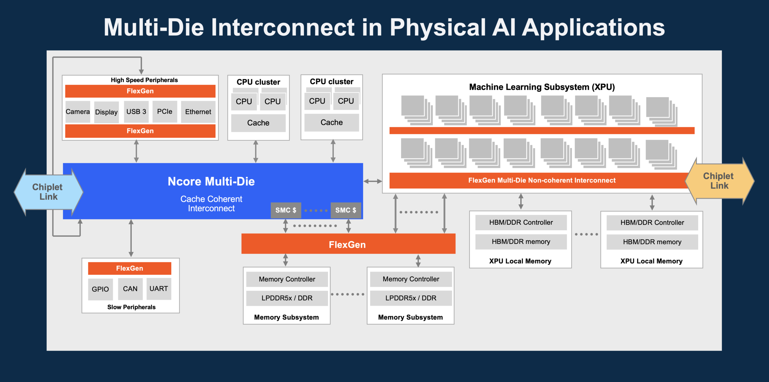
As semiconductor devices grow more complex, integrating multiple specialized dies into a single package is becoming a standard design strategy. This approach, often referred to as 3D integration or chiplet technology, allows for greater flexibility, improved yield, and the ability to mix and match different manufacturing processes. However, connecting these disparate dies poses significant challenges, particularly in maintaining high-bandwidth, low-latency communication between them. Traditional interconnects can become bottlenecks, limiting the overall performance of the multi-die system. The core problem lies in efficiently and reliably transferring data between dies that were not necessarily designed to be co-packaged, often requiring complex translation layers or proprietary interfaces.
The current landscape of multi-die systems often relies on interposer technologies or advanced packaging techniques to facilitate communication. While these methods have advanced considerably, they can introduce their own set of complexities, including increased cost, thermal management issues, and signal integrity concerns. Furthermore, the communication protocols themselves can become a point of friction. If each die uses its own internal communication fabric, bridging these different fabrics across die boundaries necessitates a translation layer, adding latency and power consumption. This is where a novel approach to Network-on-Chip (NoC) design for multi-die applications becomes critical.
A Stable Interface for Cross-Die Traffic
A new approach focuses on transporting the native packetized traffic of the NoC directly across die boundaries using a stable, invariant interface. This means that the communication protocol and packet structure remain consistent, regardless of whether the traffic is traversing within a single die or moving from one die to another within the same package. This eliminates the need for complex translation layers, significantly reducing latency and power overhead. The key innovation lies in defining an interface that can reliably carry NoC packets across the physical boundary between dies, treating the inter-die connection as just another link in the network.
This method is akin to having a universal adapter for all your electronic devices. Instead of needing different cables and converters for each type of port, you have one standard that works everywhere. In the context of multi-die systems, this stable interface acts as that universal adapter, ensuring seamless communication between any two dies that adhere to the standard. The NoC fabric itself is extended conceptually across the package, with the inter-die links acting as high-speed conduits. This simplifies the overall system architecture, making it easier to design, verify, and integrate complex multi-die products.
Benefits of a Unified Cross-Die Protocol
The advantages of this unified approach are manifold. Firstly, it dramatically simplifies the design process. Engineers can design individual dies with a standard NoC, and then integrate them into a multi-die package without needing to re-engineer the communication fabric for inter-die links. This accelerates development cycles and reduces the risk of integration errors. Secondly, the performance gains are substantial. By eliminating translation layers and directly transporting native NoC packets, latency is minimized, and bandwidth is maximized. This is crucial for applications that demand high-speed data transfer, such as advanced AI accelerators, high-performance computing, and sophisticated graphics processors.
Power efficiency is another significant benefit. Translation logic and redundant data handling are removed, leading to lower power consumption for inter-die communication. This is particularly important in power-constrained applications like mobile devices and IoT devices where every milliwatt counts. Furthermore, the stable interface promotes modularity and reusability. Chip designers can develop a library of NoC-enabled IP blocks that can be seamlessly integrated into various multi-die configurations, fostering a more robust and efficient semiconductor ecosystem. This is moving towards a more standardized approach to chiplet integration, much like how PCIe or USB became de facto standards for peripheral communication.
Implications for Future Chip Design
The implications of a stable, invariant interface for NoC traffic across die boundaries are profound. It signals a move towards more standardized and interoperable multi-die systems. As the industry increasingly adopts chiplet architectures, the need for robust and efficient inter-die communication will only grow. This approach addresses that need directly, paving the way for more complex and powerful integrated systems.
What remains to be seen is the widespread adoption of such a standard. While the technical advantages are clear, establishing an industry-wide protocol requires consensus among foundries, IP vendors, and chip designers. The long-term success will depend on its ability to be implemented cost-effectively across a range of manufacturing processes and packaging technologies. If successful, this could fundamentally alter how complex System-on-Chips (SoCs) are designed, shifting from monolithic designs to highly integrated, modular multi-die solutions that offer unprecedented flexibility and performance.