The Limits of Monolithic Design
For decades, the relentless march of Moore's Law dictated that integrated circuit performance would double approximately every two years, driven by shrinking transistor sizes on monolithic silicon dies. This approach, while immensely successful, is reaching fundamental physical and economic limits. As transistor densities increase, so do power consumption, heat dissipation challenges, and the cost of manufacturing increasingly complex single-die processors. For Artificial Intelligence (AI) workloads, which are notoriously compute-intensive and data-hungry, these limitations pose a significant bottleneck. The sheer scale of neural networks and the massive datasets they train on demand performance gains that monolithic designs struggle to deliver cost-effectively.
Enter Heterogeneous Integration and Chiplets
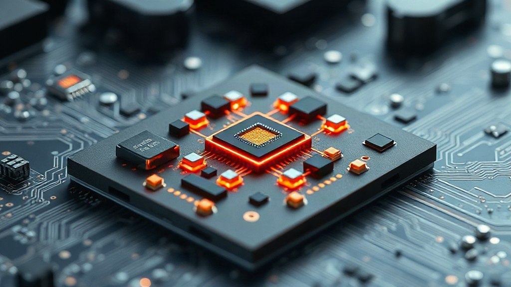
The solution gaining traction is heterogeneous integration, a paradigm shift that moves away from single, monolithic chips towards systems built from multiple, specialized chiplets. These chiplets, each optimized for a specific function – such as CPU cores, GPU cores, AI accelerators (like TPUs or NPUs), high-bandwidth memory (HBM), or I/O controllers – are interconnected on an advanced package substrate. This approach is akin to building a high-performance computing cluster not on separate motherboards, but within a single, highly integrated package. This allows designers to mix and match best-in-class IP from different foundries or internal teams, creating custom solutions tailored precisely to the demands of AI, without being constrained by the manufacturing process of a single, all-encompassing die.
Design Space Exploration Becomes Paramount
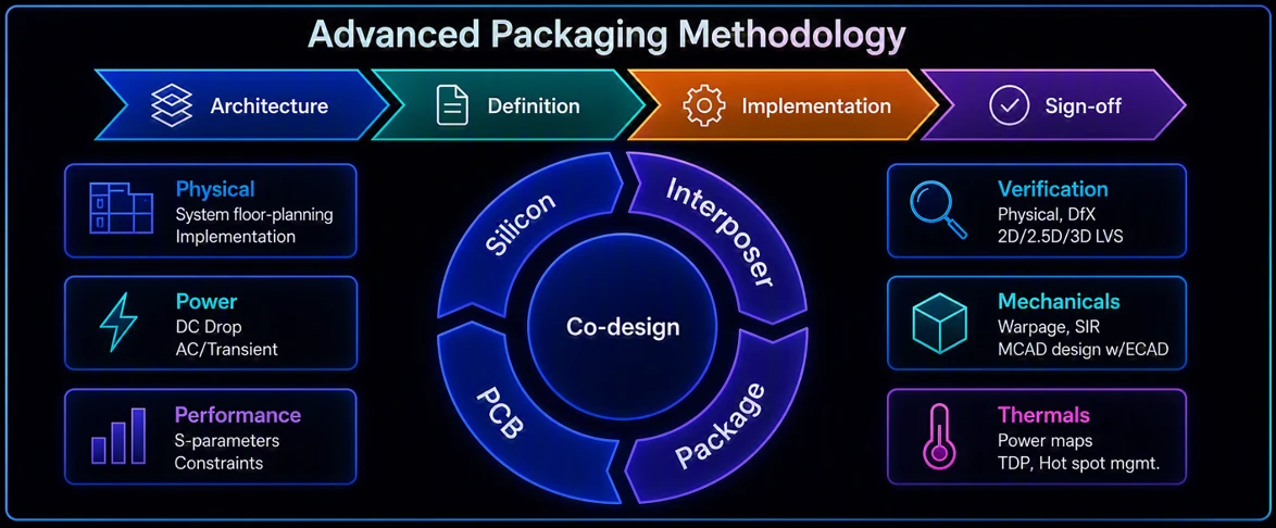
The complexity of designing these heterogeneous systems necessitates a fundamental change in the design methodology. Traditional chip design focused on optimizing a single monolithic die. With chiplet-based systems, the design space explodes. Engineers must now consider not only the design of individual chiplets but also their optimal arrangement on the package, the interconnect technologies (e.g., UCIe, AIB), the thermal management strategies for components with varying power densities, and the overall system-level performance. This requires sophisticated tools and methodologies for 'design space exploration' – a systematic process of evaluating a vast number of potential configurations to identify the optimal balance of performance, power, cost, and manufacturability. This is not merely about placing components; it's about orchestrating them for maximum synergy. Think of it less like designing a single, complex building, and more like designing a city where each specialized district (chiplet) must communicate efficiently and harmoniously with its neighbors, all within a unified infrastructure (the package).
Key Technologies Enabling Heterogeneous Integration
Several critical technologies underpin the success of heterogeneous integration for AI performance:
- Advanced Packaging Technologies: Techniques like 2.5D and 3D packaging allow chiplets to be stacked or placed side-by-side with extremely high-density interconnects, minimizing signal latency and power loss compared to traditional board-level connections. Technologies such as silicon interposers and organic substrates are crucial enablers.
- Chiplet Interconnect Standards: The development of open standards like Universal Chiplet Interconnect Express (UCIe) and proprietary solutions like Advanced Interface Bus (AIB) is vital. These standards define the physical and electrical interfaces, enabling interoperability between chiplets from different vendors. This fosters an ecosystem where specialized chiplets can be readily integrated, much like USB enabled standardized peripherals for computers.
- High-Bandwidth Memory (HBM): AI workloads require massive amounts of data to be fed to processing units rapidly. HBM, integrated directly onto the package alongside compute chiplets, provides significantly higher bandwidth and lower power consumption than traditional DDR memory, directly addressing this critical need.
- Advanced Thermal Management: Packing multiple high-performance chiplets densely creates significant thermal challenges. Novel cooling solutions, including advanced thermal interface materials and package-level cooling strategies, are essential to maintain optimal operating temperatures and prevent performance throttling.
The AI Performance Payoff
The benefits of this approach for AI are profound. By co-optimizing compute, memory, and I/O on a single package, heterogeneous systems can achieve significantly higher performance-per-watt and performance-per-area compared to monolithic designs. This translates directly into faster training times for large AI models, lower inference latency for real-time applications, and reduced overall energy consumption. Furthermore, the ability to tailor systems precisely to specific AI tasks (e.g., natural language processing, computer vision, recommendation engines) allows for greater specialization and efficiency. Companies can build custom AI accelerators that are not general-purpose but are hyper-optimized for their unique workloads, a level of customization previously unattainable or prohibitively expensive.
Challenges and the Road Ahead
Despite the immense promise, challenges remain. Ensuring the reliability and yield of complex, multi-chiplet packages is a significant hurdle. The testing and validation of such integrated systems are far more complex than for single dies. Furthermore, the ecosystem for chiplets, while growing, still requires further maturation in terms of standardization, supply chain integration, and design tool support. The economic models for chiplet design and manufacturing are also evolving, requiring new strategies for IP licensing and system integration. However, the imperative to push AI performance boundaries ensures that these challenges will be met. The future of high-performance computing, particularly for AI, is undeniably heterogeneous.