
China's Domestic Lithography Efforts Intensify
Tom's Hardware Premium this week offers an in-depth look at China's ambitious push to develop its own advanced lithography capabilities, a critical bottleneck in its pursuit of semiconductor self-sufficiency. For years, the global semiconductor industry has been dominated by a handful of companies, primarily ASML from the Netherlands, which holds a near-monopoly on the extreme ultraviolet (EUV) lithography machines essential for producing the most advanced chips. China's efforts, spurred by geopolitical pressures and a desire to reduce reliance on foreign technology, are focused on developing domestic alternatives, though significant challenges remain.
The report details the progress and hurdles faced by Chinese entities in their quest to master lithography. This is not merely about building machines; it's about mastering an intricate ecosystem of precision engineering, specialized materials, and complex software. The sheer technical complexity of lithography means that even incremental progress is a monumental undertaking. China's approach appears to be multi-pronged, involving state-backed research institutions and private enterprises, all aiming to replicate or innovate upon existing technologies. The excerpt highlights the investigative nature of this piece, suggesting a deep dive into the technical specifics and the broader strategic implications of these domestic endeavors. The implications for the global semiconductor landscape are significant, as any breakthrough in China's lithography efforts could reshape supply chains and competitive dynamics.
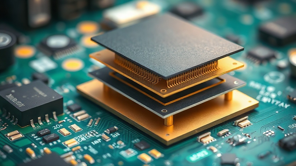
Co-Packaged Optics: The Next Frontier in Interconnects
Beyond the foundry, the premium edition also shines a spotlight on co-packaged optics (CPO), a technology poised to revolutionize how data is moved within servers and data centers. As compute demands skyrocket and chip densities increase, traditional electrical interconnects are hitting their physical limits. Signal degradation over longer distances, power consumption, and heat generation become prohibitive. Co-packaged optics aim to overcome these limitations by integrating optical transceivers directly onto the same package as the processor or switch ASIC. This proximity drastically reduces the distance data needs to travel electrically, enabling higher bandwidth, lower latency, and significantly improved power efficiency.
The article likely explores the technical underpinnings of CPO, detailing the challenges involved in manufacturing and integrating these complex components. This includes managing thermal issues, ensuring robust optical connections within a high-density package, and developing standardized interfaces. The potential benefits are immense: imagine data centers that consume less power, operate at higher speeds, and can accommodate more intensive workloads like AI training and large-scale simulations. This shift represents a fundamental change in system architecture, moving away from discrete components towards highly integrated, heterogeneous systems. The spotlight on CPO suggests a focus on its readiness for deployment, the key players in its development, and the anticipated impact on network infrastructure and high-performance computing.
Samsung Debuts Next-Generation Memory Technology
Samsung, a titan in memory manufacturing, is featured with a technical breakdown of its latest memory-related announcements. While the specifics are not detailed in the excerpt, Samsung is consistently at the forefront of memory innovation, pushing the boundaries of speed, capacity, and efficiency. This could encompass advancements in DRAM, NAND flash, or emerging memory technologies. Given the context of the other topics, it's plausible that these announcements relate to memory solutions that can support the burgeoning demands of AI, high-performance computing, and advanced networking, areas where CPO and advanced lithography play crucial roles.
The technical breakdown implies that Tom's Hardware Premium is providing readers with a detailed, perhaps even schematized, explanation of what Samsung has unveiled. This could involve new memory architectures, improved fabrication processes, or novel packaging techniques. For instance, Samsung has been a leader in High Bandwidth Memory (HBM), a type of DRAM stacked vertically and placed close to the GPU, crucial for AI accelerators. Any new iteration or alternative to HBM would be of significant interest. Similarly, advancements in NAND flash could target higher storage densities or faster read/write speeds for SSDs. The inclusion of this segment underscores the interconnectedness of the semiconductor ecosystem: without cutting-edge memory, even the most advanced processors and high-speed interconnects would be bottlenecked.
The free technical breakdown offered by Tom's Hardware Premium is a key value proposition for its subscribers. It moves beyond marketing announcements to provide a tangible understanding of the technology. This allows developers, engineers, and tech enthusiasts to grasp the practical implications of Samsung's innovations, whether it's for designing new systems, optimizing existing ones, or simply staying ahead of the curve in a rapidly evolving field. The timing of these announcements, alongside discussions on lithography and interconnects, suggests a holistic view of the future of computing hardware, from chip manufacturing to system architecture and data handling.
This week's premium content from Tom's Hardware clearly targets professionals and serious enthusiasts looking for a deeper understanding of the foundational technologies shaping the future of computing. The convergence of domestic semiconductor manufacturing efforts, advanced interconnect solutions, and next-generation memory underscores a period of intense innovation and strategic maneuvering in the global tech industry.