The Shifting Landscape of Semiconductor Testing
In the hyper-competitive semiconductor industry, where profit margins are constantly squeezed, the integrity of the test cell ecosystem has evolved from a mere operational necessity to a critical economic determinant. As dies become more complex and are integrated into increasingly expensive packages, the ability to accurately distinguish between genuine device failures and artifacts introduced by the testing process itself has become a first-order problem. This challenge underscores a fundamental shift: testing is no longer just about identifying bad chips; it's about ensuring the accuracy and reliability of the entire production outcome. The test cell, once a relatively isolated component, is now deeply intertwined with downstream processes and profitability.
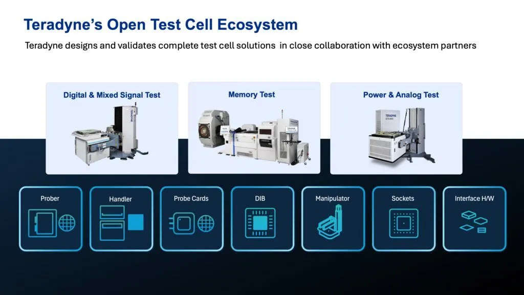
The economic stakes are immense. A single misclassified failure — an otherwise good chip marked as faulty, or worse, a faulty chip passing as good — can have cascading financial consequences. Good-die-lost (GDL) and bad-die-kept (BDK) issues directly impact yield, customer satisfaction, and brand reputation. This necessitates a holistic view of the test cell, moving beyond its individual performance metrics to understand its role within the broader test cell ecosystem. This ecosystem encompasses not only the tester itself but also the probe cards, load boards, handlers, software, and the intricate coordination between design, manufacturing, and test engineering teams.
Integration and Cross-Domain Coordination as Drivers of Outcome
The core of the modern test challenge lies in integration and cross-domain coordination. Historically, test engineers might have focused primarily on tester throughput and basic parametric measurements. However, contemporary semiconductor devices, particularly advanced System-on-Chips (SoCs) and complex memory components, demand a far more nuanced approach. These devices interact with multiple domains — analog, digital, RF, power management, and often AI acceleration blocks — each with its own unique testing requirements and potential failure modes.
Effective testing now requires a deep understanding of how these domains interact and how test stimuli might inadvertently trigger or mask failures. This means test engineers must collaborate closely with design engineers to ensure testability is built into the chip from the outset. Design for Test (DFT) strategies, including scan chains, Built-In Self-Test (BIST), and boundary scan, are no longer optional add-ons but fundamental requirements. Furthermore, the transition to advanced packaging technologies, such as 2.5D and 3D integration, introduces new testing complexities. Testing inter-chip communication, advanced interconnects like silicon interposers, and the thermal management of densely packed components requires sophisticated test methodologies and equipment that can interface with these new architectures.
The Perils of a Lying Test Cell
When the test cell 'lies'—meaning it produces inaccurate results—the consequences are severe. This can manifest in several ways. A test cell might generate false positives, leading to perfectly good chips being discarded. This is a direct hit to profitability, as valuable silicon real estate and manufacturing effort are wasted. Conversely, false negatives allow faulty chips to pass through, reaching end customers. This can result in costly field failures, warranty claims, product recalls, and, most damagingly, a severe erosion of trust in the manufacturer's quality.
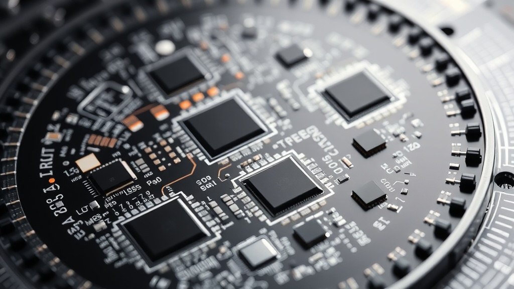
The causes of these inaccuracies are manifold. They can stem from environmental factors like temperature fluctuations or vibration, which affect the precision of measurement equipment. They can arise from worn-out or contaminated probe cards that fail to make consistent contact with the die pads. Load boards, designed to interface the tester with the device under test (DUT), can also introduce noise or signal integrity issues. Even the software controlling the test sequence can have bugs or inefficiencies that lead to incorrect test outcomes. The complexity of modern test vectors, which can run into billions of operations, also increases the likelihood of subtle errors in test pattern generation or application.
Bridging the Gap: From Tester Performance to Production Outcomes
The critical insight is that optimizing individual tester performance—such as speed or basic accuracy—is insufficient. The true measure of success is the impact on overall production outcomes. This requires a shift in focus towards the entire test cell's contribution to yield, reliability, and cost-effectiveness. This means implementing advanced data analytics and machine learning techniques to monitor test cell health, identify subtle anomalies, and predict potential failures before they impact production.
Techniques like Design for Reliability (DfR) are becoming increasingly important, integrating reliability considerations directly into the test plan. This might involve performing stress tests, accelerated life testing, or specialized characterization tests that go beyond standard functional and parametric checks. The goal is to proactively identify potential failure mechanisms that might not be apparent during standard production testing but could manifest later in the product's lifecycle. Furthermore, establishing robust feedback loops between test, manufacturing, and design teams is essential. Data from field failures, customer returns, and even early-stage production tests must be fed back to design and test engineers to refine test strategies, improve DFT, and enhance device robustness. This closed-loop approach ensures that the test cell ecosystem is not static but continuously evolving to meet the demands of increasingly sophisticated semiconductor technologies.
The Future: AI-Driven Test and Ecosystem Orchestration
The future of semiconductor testing will undoubtedly involve greater automation and intelligence. Artificial intelligence and machine learning are poised to play a significant role in optimizing test strategies, detecting complex failure patterns, and even automating test pattern generation. AI can analyze vast datasets from various test points and environmental conditions to build predictive models of device behavior and test equipment health.
This move towards intelligent automation will further emphasize the need for a well-integrated test cell ecosystem. The ability to orchestrate complex test sequences across multiple machines, adapt test parameters in real-time based on incoming data, and provide comprehensive root-cause analysis will be paramount. Companies that can successfully build and manage these sophisticated, integrated test cell ecosystems will be best positioned to navigate the economic pressures of the semiconductor market and deliver high-quality, reliable devices to their customers.