The Foundation: Understanding Semiconductor Manufacturing
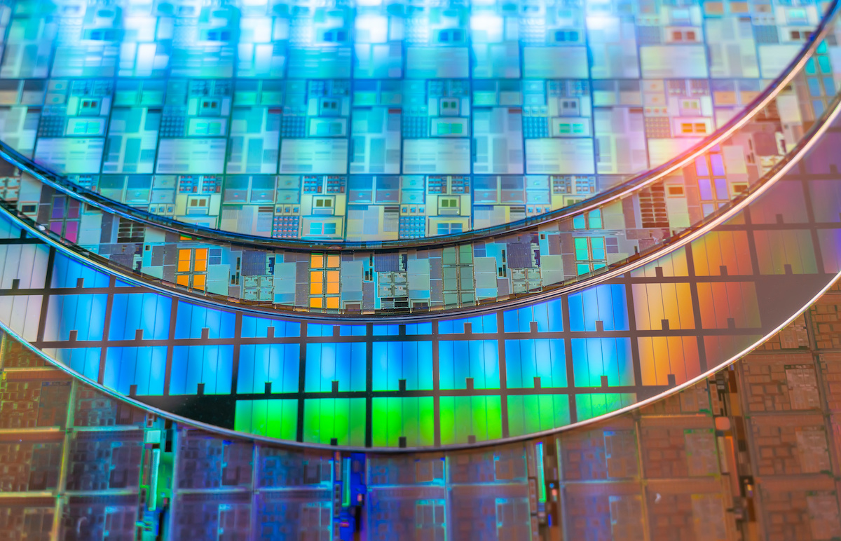
The creation of a microchip, or integrated circuit (IC), is a marvel of modern engineering. It involves an incredibly complex, multi-step process that transforms raw silicon wafers into the brains of our electronic devices. This journey from sand to silicon is characterized by extreme precision, microscopic scales, and a relentless pursuit of perfection. At its core, semiconductor manufacturing involves a series of photolithography, etching, deposition, and doping steps, all performed in highly controlled environments known as cleanrooms. The goal is to create intricate patterns of transistors and other electronic components on a wafer, which is then diced into individual chips.
The complexity arises from the sheer number of layers involved – often hundreds – each requiring exact placement and composition. Even minute deviations can render a chip useless. This demanding environment necessitates specialized equipment and advanced techniques to manage the materials used, particularly the fluids and chemicals integral to various stages of production. Precision dispensing and fluid management are not merely ancillary functions; they are critical enablers of the entire microchip manufacturing process, impacting both the front-end (wafer fabrication) and back-end (assembly and testing) operations.
Front-End Processes: Building the Circuitry
The front-end of semiconductor manufacturing is where the actual integrated circuits are built on the silicon wafer. This is the most critical and sensitive phase, involving a sequence of operations that build up and pattern the layers of material that form the transistors, interconnects, and other components. Key processes include:
- Oxidation: Growing a thin layer of silicon dioxide on the wafer surface, often used as an insulator or a mask.
- Photolithography: Transferring a circuit pattern from a mask onto the wafer surface using light-sensitive photoresist.
- Etching: Removing unwanted material from the wafer, either chemically (wet etching) or using plasma (dry etching), to define circuit features.
- Deposition: Adding thin films of various materials (metals, dielectrics, semiconductors) onto the wafer using techniques like Chemical Vapor Deposition (CVD) or Physical Vapor Deposition (PVD).
- Doping: Introducing impurities (dopants) into specific regions of the silicon to alter its electrical conductivity, typically through ion implantation or diffusion.
In these front-end stages, precision dispensing is paramount. For instance, during the application of photoresist, a uniform, defect-free coating is essential for successful lithography. Too much or too little resist, or uneven application, will lead to pattern distortions or complete failure. Similarly, during etching and cleaning steps, the exact delivery and removal of aggressive chemicals require sophisticated fluid management systems to ensure process consistency and prevent cross-contamination. Even the smallest droplet of the wrong substance, or an imprecise application of a cleaning agent, can ruin an entire wafer. The scale is so small that a single human hair is thousands of times thicker than the features being patterned.
Back-End Processes: Packaging and Integration
Once the wafer fabrication is complete, the wafer contains hundreds or thousands of individual chips, known as dies. The back-end processes involve separating these dies and preparing them for integration into final electronic products. This stage includes:
- Wafer Testing (Sort): Electrically testing each die on the wafer to identify and mark the functional ones.
- Dicing: Cutting the wafer into individual dies using high-precision saws or lasers.
- Die Attach: Mounting the functional dies onto a lead frame or substrate.
- Wire Bonding or Flip-Chip: Electrically connecting the die to the external pins of the package. This can involve fine gold or copper wires, or solder bumps for flip-chip technology.
- Encapsulation: Protecting the die and its connections with a plastic or ceramic molding compound.
- Final Test: Performing final electrical tests on the packaged chip.
Precision dispensing plays a crucial role in several back-end steps. For die attach, precise amounts of epoxy or solder paste must be dispensed to ensure secure adhesion without excess material that could interfere with subsequent processes or cause electrical shorts. In wire bonding, the placement of the wire is critical, and in flip-chip technology, the accurate placement and volume of solder bumps are vital for reliable electrical connections. Encapsulation also relies on precise dispensing of molding compounds to ensure complete coverage without voids or internal stresses that could damage the die. Fluid management is also key in cleaning processes between steps, ensuring no residue is left behind that could compromise the chip's performance or reliability.
The Role of Precision Dispensing and Fluid Management
The common thread across both front-end and back-end semiconductor manufacturing is the absolute necessity for precision dispensing and sophisticated fluid management. These systems are designed to handle a wide range of materials, from highly corrosive acids and solvents to viscous epoxies and fine solder pastes, often at micron or even nanometer scales.
Consider the challenges: materials must be dispensed with extreme accuracy in terms of volume, placement, and timing. The dispensing equipment must operate reliably in ultra-clean environments, without introducing particles or contaminants. Furthermore, the systems need to accommodate different material properties and process requirements, often requiring rapid changeovers and precise control over flow rates and pressures. Advanced dispensing technologies, such as jetting, needle dispensing, and stencil printing, are employed depending on the application's specific needs. Fluid management extends beyond dispensing to include the safe handling, storage, recycling, and waste disposal of these often hazardous chemicals, ensuring both process integrity and environmental compliance.
The surprising detail here is not the complexity of the chip itself, but the sheer intensity of the supporting infrastructure required to build it. Every single drop of chemical, every placement of a bonding wire, is controlled with a level of accuracy that would be considered impossible in most other industries. This relentless focus on precision is what allows for the miniaturization and performance gains we see in modern electronics.
Looking Ahead: The Future of Chip Manufacturing
As semiconductor devices continue to shrink and become more complex, the demands on manufacturing processes will only increase. The industry is constantly pushing the boundaries of what is possible, exploring new materials, advanced lithography techniques (like Extreme Ultraviolet, or EUV), and novel architectures. This evolution will undoubtedly place even greater emphasis on the precision and control of dispensing and fluid management systems. Innovations in areas like automation, real-time monitoring, and AI-driven process control will be crucial for maintaining yield and enabling the next generation of chips. The ability to precisely manage fluids at the nanoscale will remain a foundational pillar of progress in this dynamic field.