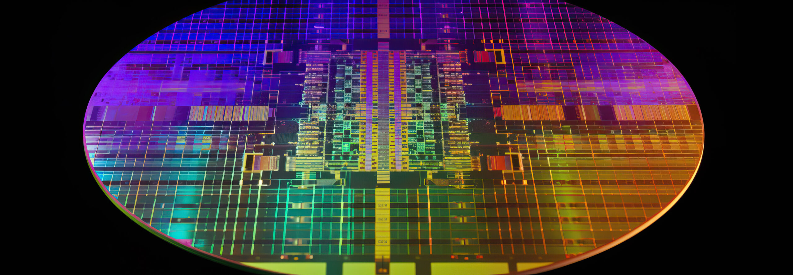
System Complexity Challenges in Modern Design
The semiconductor industry faces escalating system complexity, a challenge that permeates every stage of the design and verification process. As chips integrate more functionalities, from advanced AI processing to high-speed communication interfaces, the sheer number of components, interdependencies, and potential failure points grows exponentially. This isn't just about adding more transistors; it's about managing intricate interactions between hardware and software, ensuring robust security, and optimizing power consumption across diverse workloads. Engineers are grappling with how to effectively model, simulate, and verify these complex systems, where a bug in one module can have cascading effects throughout the entire chip. The traditional approaches to design and verification are straining under this pressure, necessitating new methodologies and tools that can handle the scale and intricacy of modern SoCs. The push towards heterogeneous integration, including 3D stacking of dies, further exacerbates these challenges by introducing new physical and electrical considerations.
Consider the analogy of building a city. In the past, you might have been designing a single, well-defined neighborhood. Now, you're responsible for an entire metropolis, complete with skyscrapers, underground transit systems, complex power grids, and a diverse population with varied needs. Each element must function independently, but also seamlessly interact with all others. A breakdown in the subway system, for instance, could cripple the entire city's economy and daily life. Similarly, a security vulnerability in one IP block could compromise the entire chip's integrity. This holistic view, once a secondary concern, is now paramount.

Advancements in Secure Ethernet for Embedded Systems
Security in networking is no longer an afterthought, especially for embedded systems that are increasingly connected. The blog review highlights the growing importance of secure Ethernet protocols. This means going beyond basic network connectivity to embed robust security mechanisms directly into the Ethernet layer. For automotive, industrial, and IoT applications, where real-time data and critical control signals are transmitted, a compromised network can have severe consequences. The focus is on implementing features like encryption, authentication, and intrusion detection at the hardware and firmware levels, making it much harder for malicious actors to intercept or manipulate data. This is particularly relevant as these systems become more distributed and interconnected, forming complex networks of devices that must communicate reliably and securely.
The challenge lies in achieving this security without significantly impacting performance or increasing power consumption, which are often tight constraints in embedded environments. Researchers and engineers are exploring lightweight cryptographic algorithms and hardware acceleration techniques to address this. The goal is to create an Ethernet implementation that is not only fast and efficient but also inherently resistant to common cyber threats, providing a trusted foundation for connected devices.
IP for 3D-ICs: Enabling Advanced Integration
Three-dimensional integrated circuits (3D-ICs) represent a significant leap in semiconductor packaging, allowing multiple dies to be stacked vertically. This approach offers benefits such as increased performance, reduced power consumption, and a smaller form factor compared to traditional planar designs. However, realizing the full potential of 3D-ICs requires specialized Intellectual Property (IP) blocks designed to handle the unique challenges of vertical integration. This includes inter-die communication interfaces, thermal management solutions, and power delivery networks that can operate efficiently across multiple stacked layers. The development of such IP is crucial for enabling next-generation applications in areas like high-performance computing, AI accelerators, and advanced mobile devices.
The integration of different process technologies and functionalities into a single 3D stack presents a complex design problem. For instance, a high-performance logic die might be stacked with a memory die, requiring extremely high-bandwidth, low-latency interconnects between them. Furthermore, managing heat dissipation becomes critical, as stacking can concentrate thermal hotspots. Specialized IP that addresses these issues, such as advanced through-silicon vias (TSVs) and sophisticated thermal sensors, is essential for the successful deployment of 3D-IC technology. This is not merely about shrinking existing designs; it's about rethinking architecture to leverage the third dimension effectively.
On-Device Gesture Recognition for Enhanced User Interfaces
The trend towards more intuitive and natural human-computer interaction is driving advancements in on-device gesture recognition. Instead of relying on cloud processing for interpreting user movements, these systems perform gesture analysis directly on the edge device, such as a smartphone, smartwatch, or smart home appliance. This approach offers significant advantages in terms of privacy, latency, and power efficiency. By keeping sensitive data local, user privacy is better protected. Lower latency means a more responsive user experience, as gestures are recognized in real-time without the delay of sending data to a remote server. Reduced power consumption is also a key benefit, crucial for battery-powered devices.
Achieving accurate and reliable gesture recognition on resource-constrained edge devices requires highly optimized algorithms and specialized hardware. This often involves leveraging machine learning models that are trained on large datasets of gestures and then compressed and quantized to run efficiently on embedded processors or dedicated AI accelerators. The accuracy must be high enough to avoid false positives and negatives, while the computational demands must be low enough to not drain the battery or introduce noticeable lag. This delicate balance is at the forefront of innovation in embedded AI and user interface design.
The MRC Protocol and Its Applications
The blog review also touches upon the Multiple Rate Congestion (MRC) protocol. While details might be scarce in a brief overview, understanding such protocols is vital for optimizing data transfer in complex networks, particularly those with varying bandwidths and potential for congestion. MRC protocols are designed to manage network traffic dynamically, adapting to changing conditions to ensure efficient and reliable data delivery. This is crucial for applications that are sensitive to latency and jitter, such as real-time video streaming, online gaming, and industrial control systems. The ability of a protocol to intelligently handle congestion and varying data rates can significantly improve user experience and system performance.
In essence, protocols like MRC act as traffic cops for data. They don't just send data packets; they actively monitor the network's capacity and adjust the flow accordingly. Imagine a highway during rush hour: a simple, unmanaged system would lead to gridlock. A well-designed protocol, like an intelligent traffic management system, reroutes traffic, adjusts speed limits, and prioritizes emergency vehicles (critical data packets) to keep things moving as smoothly as possible. The ongoing development and refinement of such protocols are essential for the continued growth of data-intensive applications and the internet of things.