
Securing Physical AI: A Growing Imperative
The rapid integration of Artificial Intelligence (AI) into hardware, particularly for edge devices and specialized accelerators, brings a new set of security challenges. While software-based AI security has seen significant attention, the physical implementation of AI models within silicon is increasingly becoming a critical vulnerability. This July, Semiconductor Engineering highlighted the growing need to secure physical AI. This isn't just about protecting intellectual property; it's about ensuring the integrity and trustworthiness of AI systems that may control critical infrastructure, autonomous vehicles, or sensitive data processing.
Attacks on physical AI could range from sophisticated side-channel attacks that infer model parameters to more direct hardware Trojans designed to subtly alter AI decision-making. The complexity of modern AI models, often involving vast neural networks with billions of parameters, makes them inherently difficult to audit and secure. Furthermore, the trend towards specialized AI hardware, including custom ASICs and FPGAs, means that security solutions must be tailored to specific architectures. The challenge lies in developing robust defense mechanisms that can be integrated early in the design cycle, without significantly impacting performance or power consumption. This requires a multidisciplinary approach, bridging the gap between AI researchers, hardware designers, and security experts. The focus is shifting from securing the data fed to the AI to securing the AI itself as a physical entity.

The Crucial Role of Feedback in Agent Development
AI agents, designed to perform tasks autonomously, are only as good as the feedback they receive. July’s blog review underscored the importance of effective feedback mechanisms for training and refining these agents. Whether agents are learning to navigate complex environments, manage resources, or interact with users, continuous and relevant feedback is paramount. This feedback loop is essentially the agent's learning mechanism. Without it, or with poor-quality feedback, agents can become stuck in suboptimal behaviors, fail to generalize to new situations, or even exhibit undesirable emergent properties.
The nature of the feedback is as critical as its presence. Sparse rewards, delayed feedback, or noisy signals can significantly hinder learning efficiency. Developers are exploring various strategies to optimize this process, including reinforcement learning techniques that reward desired behaviors and penalize undesired ones, imitation learning where agents learn from expert demonstrations, and meta-learning approaches that allow agents to adapt their learning strategies based on past experiences. The challenge is to design feedback systems that are informative, timely, and scalable, especially as agents tackle increasingly complex tasks. Think of it less like a teacher giving a single grade at the end of a semester, and more like a coach providing real-time, actionable advice during a game. This granular, continuous feedback is what enables agents to truly master their domains.
3D-IC Security: Addressing New Frontiers
As the semiconductor industry pushes the boundaries of integration with 3D Integrated Circuits (3D-ICs) and advanced packaging techniques, new security vulnerabilities emerge. The July review pointed to the unique security concerns associated with stacking multiple dies vertically. In a traditional 2D chip, interconnections are primarily on the same plane. In 3D-ICs, however, dies are stacked and interconnected through through-silicon vias (TSVs) or micro-bumps, creating a more complex interconnect fabric.
This increased complexity introduces new potential attack surfaces. For instance, malicious actors might attempt to exploit the TSVs to inject false data, eavesdrop on inter-die communication, or even induce physical damage. Securing 3D-ICs requires a holistic approach, considering not only the security of individual dies but also the integrity of the connections between them. This involves architectural-level security features, secure design methodologies, and robust testing procedures throughout the manufacturing process. The ability to isolate critical functions or data across different stacked dies, and to verify the integrity of data as it traverses these vertical interconnects, becomes essential. The industry is grappling with how to standardize security measures for these complex multi-die systems, ensuring that the benefits of advanced packaging do not come at the cost of compromised security.
Chiplet Interoperability: Standards for a Modular Future
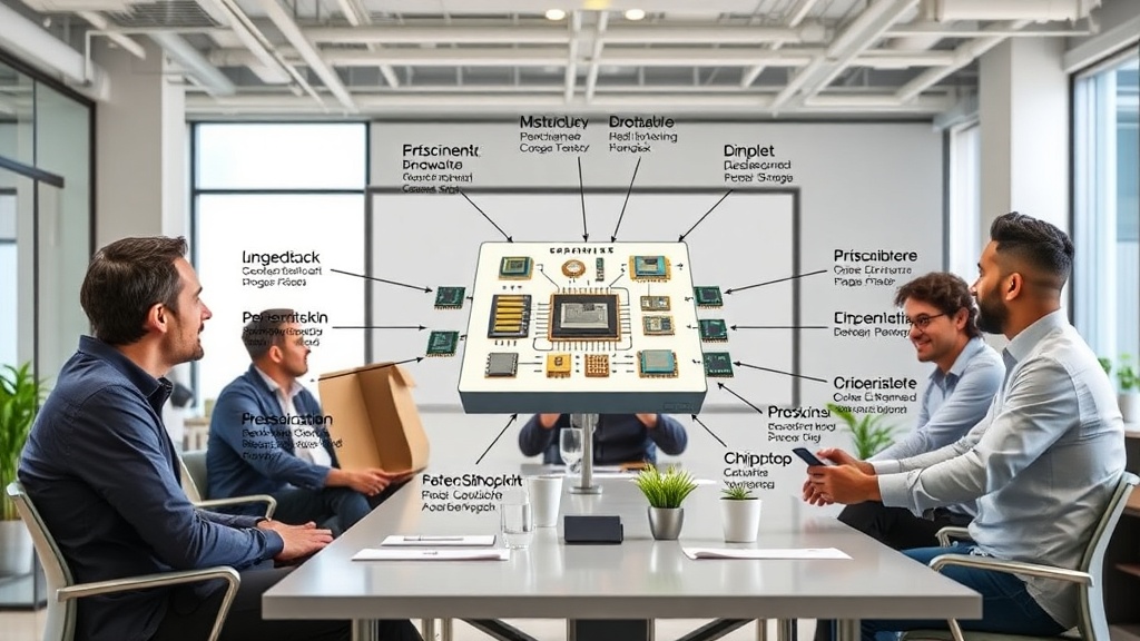
The rise of chiplets – standardized, smaller semiconductor dies that can be combined in a package to form a larger system – promises greater design flexibility, cost efficiency, and faster time-to-market. However, realizing this modular future hinges on seamless interoperability between chiplets from different vendors. July's discussions touched upon the critical need for robust standards that govern how these chiplets communicate and function together.
Without agreed-upon interfaces and protocols, the chiplet ecosystem risks fragmentation and vendor lock-in, undermining its core value proposition. Standards bodies and industry consortia are working on defining these interfaces, covering aspects like physical connectivity, electrical signaling, and communication protocols. Achieving true interoperability means that a CPU chiplet from one company should, in principle, be able to work with a GPU or I/O chiplet from another, provided they adhere to the established standards. This is akin to the USB standard for peripherals; you can plug in a mouse from one manufacturer and a keyboard from another, and they just work. The success of the chiplet revolution depends on achieving this level of plug-and-play compatibility across the semiconductor supply chain.
RF Digital Twins for Enhanced Design and Validation
The complexity of Radio Frequency (RF) designs, especially for advanced communication systems like 5G and beyond, presents significant validation challenges. The blog review highlighted the application of digital twins in the RF domain. A digital twin is a virtual replica of a physical asset, process, or system, updated with real-time data. For RF systems, a digital twin can model the behavior of components, circuits, or even entire systems, allowing for extensive simulation and analysis without the need for physical prototypes at every stage.
This approach enables designers to explore a wider range of design parameters, test performance under various environmental conditions, and predict potential failure modes much earlier in the design cycle. It’s like having a highly sophisticated flight simulator for your chip design, allowing you to test every conceivable scenario before the actual aircraft (or chip) ever leaves the ground. The accuracy of the digital twin is crucial, relying on high-fidelity models derived from measurement data and electromagnetic simulations. The integration of AI and machine learning further enhances the predictive capabilities of these RF digital twins, making them powerful tools for accelerating innovation and improving the reliability of next-generation wireless technologies.