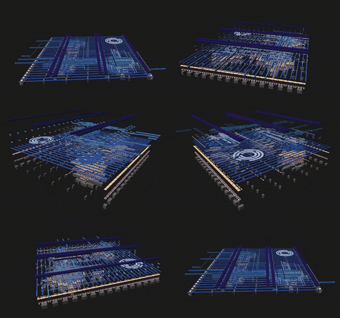
The Challenge of ASIC Reverse Engineering
The idea of reverse engineering an Application-Specific Integrated Circuit (ASIC) is captivating, conjuring images of determined engineers dissecting proprietary hardware to uncover its secrets. However, the reality is far removed from simple software decompilation. ASICs are custom-designed chips, built from the ground up for a specific function, often with significant intellectual property protection embedded within their physical structure and design files. This makes them inherently difficult to reverse engineer.
Unlike Field-Programmable Gate Arrays (FPGAs) or microcontrollers, which offer some level of programmability or accessible instruction sets, ASICs are fixed-function devices. Their logic is permanently etched into silicon. This means that any attempt at reverse engineering must contend with the physical manifestation of the design, rather than an abstract code representation. The process is less about reading software and more about deciphering a physical blueprint at a microscopic level.
Why Reverse Engineer an ASIC?
The motivations for undertaking such a formidable task can vary:
- Security Auditing: To identify potential backdoors, hardware Trojans, or vulnerabilities in critical security hardware. This is particularly relevant for government or defense applications.
- Intellectual Property Theft: Competitors might attempt to steal designs to replicate or improve upon them, though this is illegal and ethically dubious.
- Legacy System Maintenance: When original design documentation is lost or unavailable, reverse engineering might be the only way to understand and maintain obsolete hardware.
- Academic Research: For understanding cutting-edge fabrication techniques, circuit design principles, or the evolution of hardware security.
- Debugging and Analysis: To understand unexpected behavior or performance issues in complex integrated systems.
Each of these scenarios presents unique challenges and demands different levels of detail and accuracy from the reverse engineering process.
The Multi-Stage Process
Reverse engineering an ASIC is not a single step but a complex, multi-stage process that requires specialized equipment, deep expertise, and significant time. It can generally be broken down into several key phases:
1. Physical Decapsulation and Delayering
The first hurdle is accessing the silicon die itself. This involves removing the chip's packaging without damaging the delicate circuitry within. Techniques include chemical etching, laser ablation, or precise mechanical removal. Once decapsulated, the chip must be carefully delayered, removing successive layers of metal interconnects and dielectric material to expose the underlying transistors and logic gates. This is often done using focused ion beam (FIB) milling or precise chemical etching, layer by layer.
2. Imaging and Feature Extraction
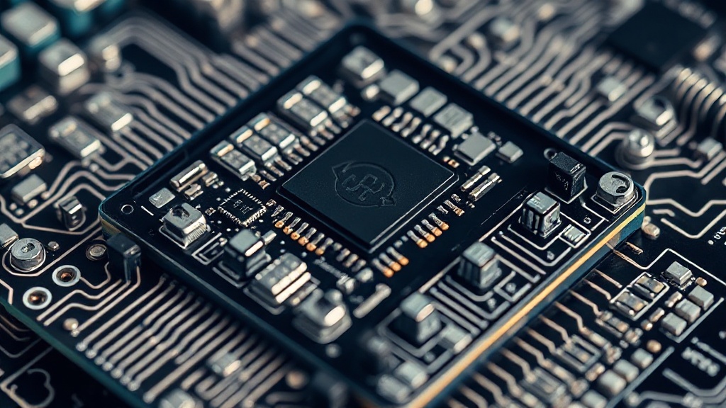
As layers are removed, high-resolution imaging techniques are employed. Scanning Electron Microscopy (SEM) is crucial for capturing detailed images of the transistors, wires, and other features at the nanometer scale. Optical microscopy might be used for coarser layers. These images form the basis for reconstructing the circuit's layout.
3. Netlist Extraction and Reconstruction
The extracted images are then processed by specialized software. This software attempts to identify individual components (transistors, capacitors, resistors) and their interconnections. This process, known as netlist extraction, is highly automated but requires significant manual verification and correction. The goal is to generate a logical representation of the circuit, often in a hardware description language (HDL) format like Verilog or VHDL, that can be simulated and analyzed.
4. Functional Verification and Analysis
Once a netlist is reconstructed, it must be verified against the original chip's behavior. This involves creating test vectors and simulating the extracted netlist to see if it produces the same outputs for given inputs as the actual ASIC. This is a critical and often iterative step. If the simulation doesn't match the real-world behavior, the extraction process must be revisited. Analyzing the functionality helps understand what the circuit actually does, beyond just its structure.
Practical Limitations and Impracticality
While the process is technically feasible, its practicality is severely limited. The primary barriers are:
- Cost: The specialized equipment (FIB, SEM, advanced chemical etchants), software, and highly skilled personnel required are exceptionally expensive. A single FIB machine can cost hundreds of thousands, if not millions, of dollars.
- Time: Reverse engineering even a moderately complex ASIC can take months or even years. Each layer of delayering and imaging, and subsequent netlist extraction and verification, is time-consuming and prone to error.
- Complexity: Modern ASICs contain billions of transistors. Manually tracing and reconstructing the logic for such dense circuits is an almost insurmountable task. Automation helps, but human oversight and expertise are indispensable.
- Design Obfuscation: Chip designers employ various techniques to make reverse engineering more difficult. These can include intentionally confusing layout, redundant logic, or even intentionally placed