The Challenge of Wide-Bandgap Semiconductor Defects
The semiconductor industry's relentless pursuit of higher performance, efficiency, and power density has driven a significant shift towards wide-bandgap (WBG) materials like Silicon Carbide (SiC) and Gallium Nitride (GaN). These materials enable devices that operate at higher voltages, temperatures, and frequencies than traditional silicon, making them crucial for applications ranging from electric vehicles and renewable energy systems to advanced power electronics and high-frequency communications. However, manufacturing WBG devices presents unique challenges, particularly in detecting and mitigating defects that can severely impact device performance and reliability.
One of the primary hurdles is the presence of subsurface or crystalline defects. These imperfections, often invisible to standard surface inspection techniques, can create leakage paths, degrade breakdown voltage, and lead to premature device failure. Traditional methods like optical microscopy or X-ray diffraction are often insufficient for pinpointing these deep-seated issues, especially in the complex crystal structures of SiC and GaN. This gap in inspection capability directly translates to reduced manufacturing yields and increased costs.
Photoluminescence Inspection: A Deeper Look
Photoluminescence (PL) inspection is emerging as a powerful solution to this critical manufacturing challenge. Unlike surface-sensitive techniques, PL works by exciting the semiconductor material with a light source (typically a laser) and then analyzing the light emitted by the material as it relaxes. This emitted light, or photoluminescence, carries specific spectral signatures that are directly related to the material's electronic band structure and the presence of various impurities or defects. By studying the intensity, wavelength, and decay time of the emitted light, manufacturers can gain unprecedented insights into the material's quality.
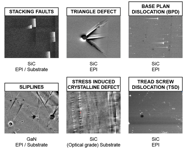
For SiC and GaN, PL inspection is particularly effective at identifying defects that affect electrical behavior. These can include point defects, dislocations, stacking faults, and impurities. For example, certain point defects in SiC can lead to deep energy levels within the bandgap, acting as recombination centers or trapping sites for charge carriers. These defects can manifest as specific peaks or quenching in the PL spectrum. Similarly, in GaN, the presence of dislocations can influence the material's luminescence properties, providing a way to map their distribution and density across the wafer.
The advantage of PL lies in its ability to probe beneath the surface. The excitation light can penetrate a certain depth into the material, and the subsequent luminescence originates from within that volume. This allows for the detection of subsurface defects that would otherwise go unnoticed until later stages of device fabrication or, worse, after the device is in the field. This early detection is key to protecting yield.
Automating Defect Detection for High-Volume Manufacturing
To be effective in high-volume manufacturing environments, PL inspection systems must be fast, accurate, and automatable. Modern PL inspection tools integrate advanced optical systems, high-sensitivity detectors, and sophisticated algorithms for data analysis. Lasers of varying wavelengths can be used to probe different depths and material properties. Spectrometers can capture the full emission spectrum, while spatially resolved PL mapping allows for the visualization of defect distribution across the entire wafer or even within individual die.
The automation aspect is crucial. Manual inspection is impractical for the speeds and scales required in semiconductor foundries. Automated PL systems can perform full wafer scans in minutes, comparing the obtained spectra and intensity maps against established quality standards. Any deviation triggers an alert, enabling engineers to take corrective action. This could involve adjusting process parameters, identifying faulty equipment, or quarantining affected batches of material.
The integration of PL inspection into the manufacturing workflow provides a feedback loop that is essential for continuous process improvement. By correlating PL data with downstream electrical test results, manufacturers can refine their understanding of how specific defects impact device performance. This allows for the development of more precise process control strategies and the optimization of material growth and device fabrication steps.
Beyond Basic Defect Detection: Advanced Applications
The capabilities of PL inspection extend beyond simple defect identification. Advanced techniques are being developed to extract even more nuanced information. For instance, time-resolved photoluminescence (TRPL) measures the decay time of the emitted light, which is highly sensitive to the concentration and type of defects acting as recombination centers. Faster decay times often indicate a higher density of defects that efficiently quench luminescence.
Furthermore, by using different excitation wavelengths and analyzing the resulting emission, it's possible to differentiate between various types of defects and their locations within the material. This spectral deconvolution allows for a more precise characterization of the material's electronic landscape. For applications requiring extreme uniformity, such as high-power SiC MOSFETs or GaN HEMTs, detailed PL mapping can reveal subtle variations in material quality that might otherwise lead to inconsistent device performance across a wafer.
The surprising detail here is not just the ability to see defects, but the precision with which PL can differentiate between defect types. It's not a blunt instrument; it's a highly refined diagnostic tool that provides a fingerprint of the material's internal state. This level of detail is what enables manufacturers to move from simply detecting problems to actively engineering solutions.
The Future of WBG Device Manufacturing
As the demand for SiC and GaN devices continues to surge, driven by the global push for electrification and energy efficiency, the importance of robust yield protection strategies cannot be overstated. Photoluminescence inspection represents a significant advancement in this area. By providing a non-destructive, highly sensitive method for detecting critical subsurface and crystalline defects, PL inspection empowers manufacturers to improve device quality, increase yields, and reduce the overall cost of WBG semiconductors.
This technology is not merely an incremental improvement; it is fundamentally changing how manufacturers approach quality control for these advanced materials. The ability to gain deep, actionable insights into the material's electronic properties early in the fabrication process is critical for unlocking the full potential of SiC and GaN technologies. As PL systems become more sophisticated and integrated, they will play an even larger role in ensuring the reliability and performance of the next generation of power and high-frequency electronic devices.