
Advancements in Semiconductor Interfaces and Materials
Recent technical papers highlight critical advancements in understanding and manipulating semiconductor interfaces. One key area of focus is the behavior of Schottky barriers at Si/metal interfaces. These barriers play a crucial role in the performance of various semiconductor devices, including diodes, transistors, and solar cells. Precise control over their formation and characteristics is essential for optimizing device efficiency and reliability. Researchers are exploring novel materials and deposition techniques to engineer these interfaces, aiming to reduce contact resistance and improve carrier injection/extraction properties. Understanding the quantum mechanical effects at play, such as tunneling and thermionic emission, is paramount for designing next-generation interconnects and contacts that can withstand increasing current densities and thermal loads in advanced chip architectures.
Further exploration into material science extends to the realm of photonic integrated circuits (PICs). A significant challenge in this domain is robust hardware fingerprinting, which is vital for intellectual property protection and counterfeit detection. New research is investigating methods for uniquely identifying photonic ICs, potentially through analyzing their specific optical responses or fabrication variations. This involves developing sophisticated measurement techniques and algorithms that can distinguish between nominally identical devices, accounting for the inherent variability in photonic manufacturing processes. The goal is to create a secure and verifiable identity for each chip, ensuring its authenticity throughout the supply chain.
Agentic AI and Hardware Design Automation
The integration of Artificial Intelligence (AI) into hardware design is accelerating, with a particular emphasis on agentic approaches. One paper examines agentic High-Level Synthesis (HLS), a technique that aims to automate the conversion of high-level programming languages (like C/C++) into hardware descriptions (like Verilog/VHDL). Agentic HLS involves intelligent agents that can learn and adapt their synthesis strategies based on the specific design and target performance metrics. This moves beyond traditional, rule-based HLS compilers by incorporating machine learning to optimize for factors such as area, power, and timing more effectively. The agents can explore a vast design space, making informed decisions about microarchitecture choices, scheduling, and resource allocation, thereby potentially achieving better results than manual design or conventional automated tools.
Complementing this, another paper discusses agentic hardware design automation as a form of repository-level code evolution. This perspective views the entire hardware design process, including IP integration and verification, as a continuously evolving system managed by intelligent agents. These agents could be responsible for tasks such as identifying design flaws, suggesting optimizations, managing version control, and even automatically generating test cases. The concept of repository-level code evolution implies a more holistic and autonomous approach to hardware development, where AI agents not only assist in specific design tasks but also contribute to the overall improvement and maintenance of the design codebase over time. This could drastically reduce the design cycle time and improve the quality of complex System-on-Chips (SoCs).
Probabilistic Memory for Edge Computing and RISC-V Platforms
The demands of edge computing, characterized by resource constraints and the need for low-power operation, are driving innovation in memory architectures. One paper introduces probabilistic memory concepts tailored for edge devices. Unlike traditional deterministic memory, probabilistic memory may have a certain chance of errors, but this error rate can be managed and exploited. For applications where occasional data corruption is tolerable or can be corrected with lightweight error detection/correction codes, probabilistic memory can offer significant advantages in terms of power consumption and density. This is particularly relevant for AI inference at the edge, where the precise accuracy of every single bit might not be critical for overall task performance. Researchers are exploring how to design and utilize such memories to achieve a better trade-off between reliability, performance, and energy efficiency.
In parallel, the open-source RISC-V architecture continues to gain momentum, fostering innovation in customizable hardware platforms. A paper highlights the development of an open-source, customizable RISC-V SoC platform. Such platforms are crucial for enabling rapid prototyping and specialized hardware development without the high costs associated with proprietary architectures. By providing a flexible and modular RISC-V-based SoC, researchers and developers can easily integrate custom accelerators, peripherals, and memory subsystems. This fosters a collaborative ecosystem where novel architectures and applications can be explored and validated quickly. The availability of such platforms accelerates the adoption of RISC-V for a wide range of applications, from embedded systems and IoT devices to high-performance computing and AI accelerators.
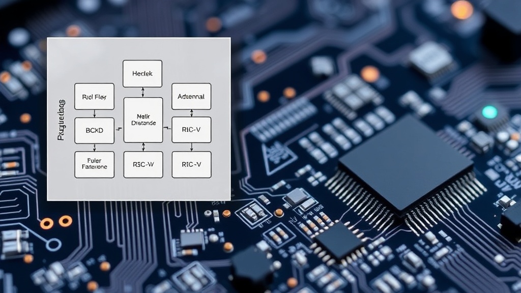
These diverse research efforts underscore a broader trend in the chip industry: the push towards greater intelligence and autonomy in both hardware design and device operation, coupled with a growing reliance on open standards and specialized architectures. From the fundamental physics of material interfaces to the high-level automation of design processes and the efficient deployment of AI at the edge, the papers collectively point towards a future of more sophisticated, efficient, and accessible semiconductor technologies.