
Cerebellum-Inspired Memristor Architectures
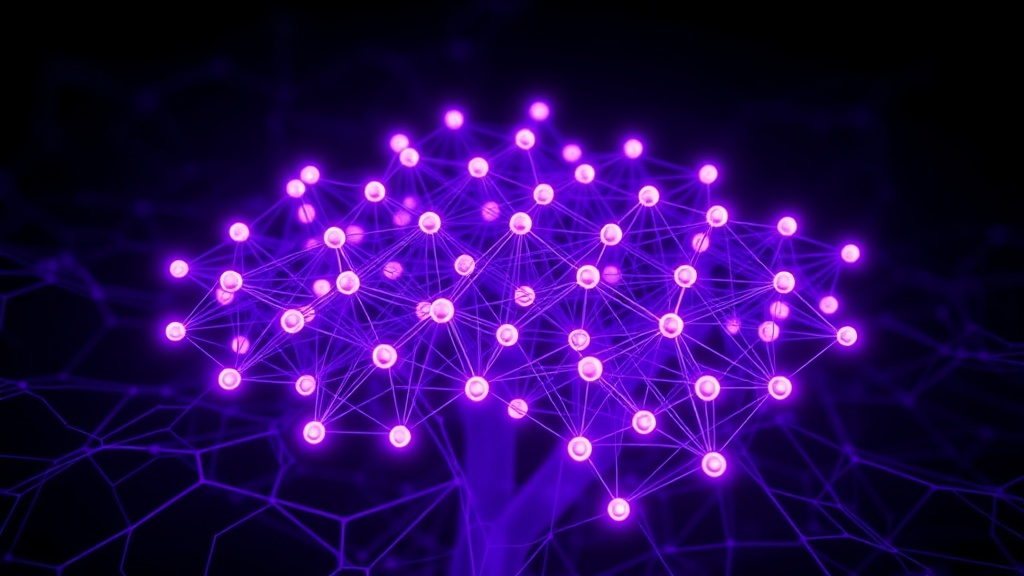
Researchers are developing novel memristor devices inspired by the human cerebellum, aiming to mimic its efficient information processing capabilities. This approach leverages the unique properties of memristors, which can change their resistance based on the history of the voltage applied across them, analogous to synaptic plasticity in biological neurons. The cerebellum is known for its role in motor control, coordination, and learning, processing vast amounts of sensory input in parallel with remarkable energy efficiency. By architecting memristor arrays in a manner that reflects the cerebellar microcircuitry, specifically the granular layer and Purkinje cells, scientists hope to create neuromorphic hardware that can perform complex computations with significantly lower power consumption than traditional von Neumann architectures.
The core idea is to move beyond simple artificial neurons and synapses towards more complex, biologically plausible computational units. Early research suggests that these cerebellum-inspired designs can exhibit improved performance in tasks like pattern recognition and sequence learning. The key challenge lies in fabricating these complex 3D structures reliably and at scale, as well as developing the algorithms that can effectively harness their unique computational properties. This research could pave the way for more sophisticated AI hardware, capable of handling real-time sensory data processing for applications ranging from autonomous systems to advanced prosthetics.
Fungal Mycelium as a Sustainable PCB Substrate
A significant hurdle in electronics manufacturing is the environmental impact of traditional materials, particularly the fiberglass and epoxy resins used in printed circuit boards (PCBs). A promising alternative emerging from recent research is the use of fungal mycelium, the root-like structure of fungi, as a biodegradable substrate for PCBs. Mycelium can be grown on agricultural waste, effectively upcycling discarded materials into a dense, robust matrix. This mycelial material can then be processed and shaped into a substrate suitable for mounting electronic components.
The process typically involves inoculating a substrate like sawdust or straw with fungal spores and allowing the mycelium to grow and bind the particles together. Once a desired density and shape are achieved, the growth is halted, often through heat treatment, resulting in a stable and lightweight material. This material exhibits good insulating properties and can be modified to accept conductive traces, either through direct printing methods or by incorporating conductive fillers. While the electrical conductivity and thermal management capabilities of mycelium-based PCBs are still areas of active research and development, their potential for a drastic reduction in e-waste and reliance on petrochemicals is substantial. This innovation aligns with a broader push towards circular economy principles in the electronics industry, offering a glimpse into a future where electronic devices are not only functional but also environmentally benign throughout their lifecycle.
Advancements in Doping Organic Semiconductors
The performance of organic semiconductors, which are crucial for flexible displays, organic photovoltaics, and certain types of sensors, is heavily reliant on precise doping. Doping introduces impurities into the semiconductor material to control its electrical conductivity, a process that has historically been more challenging and less effective with organic materials compared to their inorganic counterparts like silicon. Recent research has focused on developing new doping strategies and materials that offer greater control, stability, and efficiency.
One area of focus is the development of novel p-type and n-type dopants that are more compatible with a wider range of organic semiconductor molecules. Traditional dopants can sometimes degrade the organic material or lead to undesirable side reactions. New approaches involve using molecular dopants that form stronger, more stable charge-transfer complexes, or employing electrochemical doping techniques that allow for in-situ tuning of conductivity without introducing permanent chemical impurities. Another avenue explores the use of dopants that can self-assemble within the organic matrix, leading to more uniform conductivity profiles. These advancements are critical for unlocking the full potential of organic electronics, enabling higher performance, longer device lifetimes, and broader applicability in consumer electronics and beyond. The ability to fine-tune the electronic properties of organic materials with greater precision will be key to their wider adoption in next-generation electronic devices.