The Challenge of Backside Power Delivery
As semiconductor devices shrink and packing density increases, managing power delivery becomes a critical bottleneck. Backside power delivery networks (BSPDN) offer a promising solution by moving power delivery to the backside of the wafer, freeing up valuable space on the active front side for logic and memory. This approach allows for shorter interconnects and improved performance. However, the physical implementation of BSPDN involves complex structures, including Through-Silicon Vias (TSVs), which connect the frontside to the backside, and Backside Power Rails (BPRs) that distribute power. A key challenge lies in the interface between the nano-TSVs and the BPRs. Any imperfections or suboptimal geometries at this connection point can lead to increased resistance, voltage droop, and reduced power efficiency, directly impacting device performance and reliability.
The intricate nature of these nano-scale connections means that traditional analytical models often fall short. Small variations in manufacturing processes, such as the rounding of corners during etching, can have disproportionately large effects on electrical performance. Understanding and mitigating these effects is paramount for realizing the full potential of advanced packaging technologies like 3D integration and heterogeneous integration.
Virtual Modeling for Precision Analysis
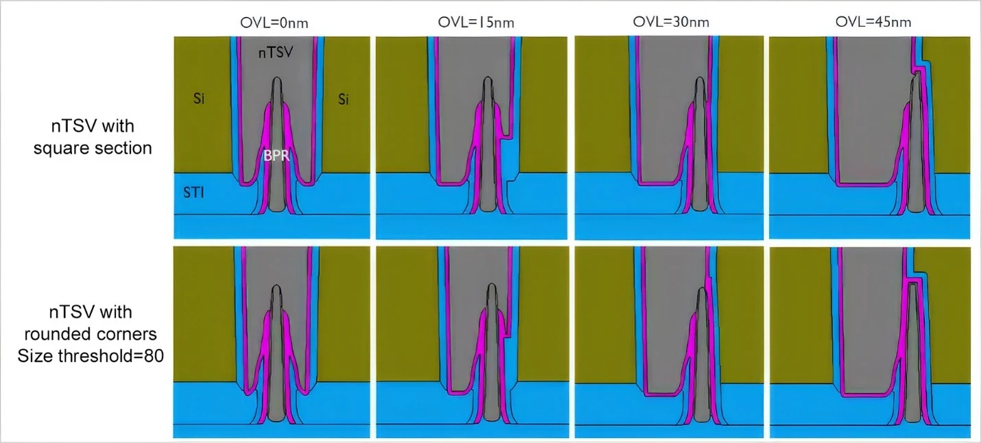
To address these challenges, researchers have developed a realistic virtual model to meticulously analyze the nano-TSV-to-BPR connection. This model goes beyond simplified geometric assumptions to capture the nuanced physical realities of semiconductor fabrication. Specifically, it investigates the impact of rounded corners on the TSV sidewalls and their resulting influence on the resistance experienced at the connection point. Resistance here is not just a simple bulk material property; it's heavily influenced by the precise geometry of the current path.
The virtual model simulates the flow of current through the TSV and into the BPR. By varying the degree of corner rounding, from sharp, idealized edges to significantly rounded profiles, the simulation quantifies the resultant change in electrical resistance. This allows engineers to see, with a high degree of accuracy, how manufacturing variations translate directly into performance degradation. The sensitivity analysis performed by this model is crucial because it highlights which geometric parameters are most critical to control during fabrication to achieve optimal electrical performance.
The Surprising Impact of Rounded Corners
The most significant finding from this modeling effort is the surprisingly substantial impact that seemingly minor corner rounding can have on the effective resistance of the nano-TSV-to-BPR connection. While one might intuitively expect a slight increase in resistance due to a longer effective path, the simulations reveal that the effect is often non-linear and can be exacerbated by the specific dimensions and materials involved. Rounded corners can alter the current density distribution, leading to localized hotspots and further increases in effective resistance. This phenomenon is akin to trying to pour water through a pipe with a very smooth, gradual bend versus a sharp, abrupt one – the resistance to flow is different, and in the electrical case, it’s the resistance to electron flow that matters.
This counterintuitive finding underscores the need for advanced simulation tools that can accurately predict the electrical behavior of these complex structures. It moves the focus from simply achieving the target dimensions to understanding the tolerance of the design to process variations. The model demonstrates that even a few nanometers of rounding can push the connection's resistance beyond acceptable thresholds, particularly in high-performance applications where every milliohm of resistance counts.
Optimization Strategies and Future Directions
Based on the insights gained from the virtual model, several optimization strategies can be employed. Firstly, process engineers can refine etching and deposition techniques to minimize corner rounding during TSV formation and BPR integration. This might involve adjusting plasma parameters, optimizing mask designs, or employing advanced deposition methods that conform better to complex geometries.
Secondly, designers can incorporate design rules that account for this sensitivity. This could mean specifying a larger BPR footprint where it interfaces with the TSV, or even subtly altering the TSV geometry to be more tolerant to corner rounding. The virtual model serves as a powerful tool for design space exploration, allowing engineers to test various design modifications virtually before committing to costly silicon fabrication. This iterative design-build-test cycle is significantly accelerated by accurate simulation.
The long-term implication of this work is the advancement of more robust and efficient backside power delivery networks. As chiplets and advanced packaging become more prevalent, the ability to precisely control and optimize these critical interconnects will be a key differentiator for semiconductor manufacturers. Further research could explore the impact of different materials, TSV aspect ratios, and the interaction between multiple TSVs in dense arrays, all guided by sophisticated virtual modeling techniques.