The Scale of Ambition: Terafab's Mammoth Footprint
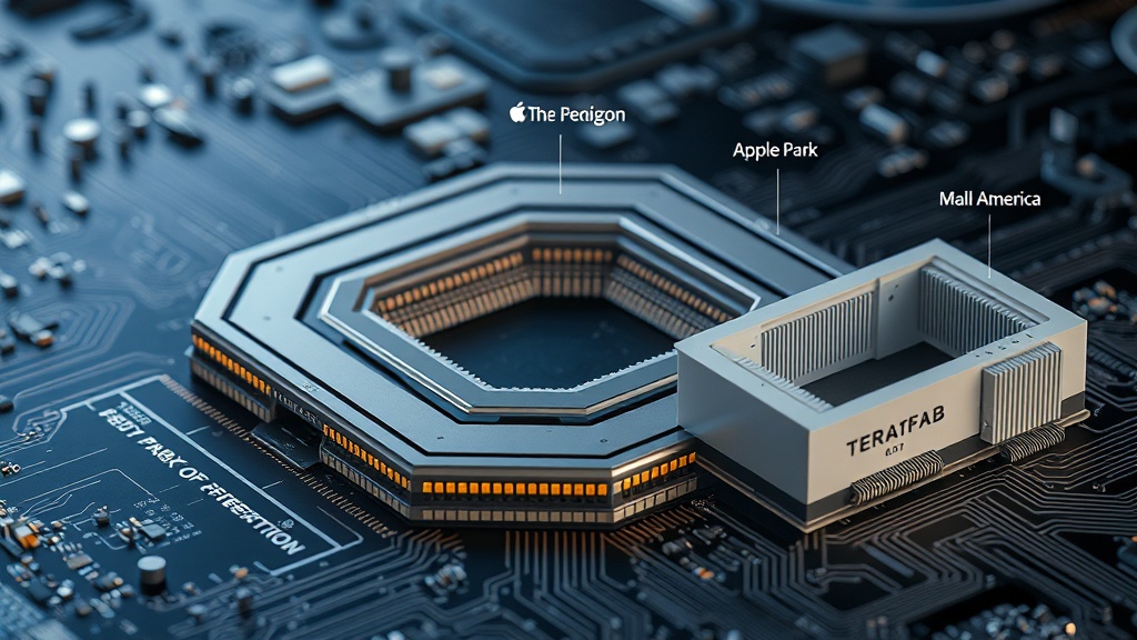
Elon Musk's vision for a fully integrated semiconductor manufacturing facility, dubbed Terafab, is shaping up to be an undertaking of unprecedented scale. Preliminary projections suggest an interior space of at least 100 million square feet. To put this into perspective, this single facility would dwarf some of the most iconic and expansive structures on the planet. Consider the Pentagon, the headquarters of the U.S. Department of Defense, which spans approximately 6.5 million square feet. Apple Park, Apple's futuristic corporate campus, covers about 2.8 million square feet. Even the Mall of America, one of the largest shopping malls in North America, encompasses roughly 5.6 million square feet of gross leasable area. Musk's own Giga Texas, a sprawling electric vehicle factory, is itself a massive industrial complex. When combined, these landmarks represent a colossal amount of built space, yet Musk's Terafab is projected to surpass their aggregate footprint by a significant margin.
This sheer magnitude is not merely for show; it is a direct consequence of Musk's audacious plan to consolidate multiple, complex semiconductor manufacturing processes under a single roof. Traditional semiconductor fabrication plants, or fabs, are already enormous, state-of-the-art facilities requiring vast amounts of space for cleanrooms, intricate machinery, R&D labs, logistics, and support infrastructure. However, Terafab aims to go further, integrating not just the core fabrication of chips but potentially precursor material production, advanced packaging, testing, and even R&D for next-generation chip architectures. This all-in-one approach necessitates a scale that current industry leaders have not pursued, reflecting a fundamental rethinking of how semiconductors are designed and manufactured.
The 'All-in-One' Manufacturing Model
The core innovation behind Terafab lies in its ambition to be a truly integrated, end-to-end semiconductor factory. Today, the semiconductor supply chain is highly specialized and geographically dispersed. Chip design often happens in one location (e.g., Silicon Valley), wafer fabrication in another (often in Taiwan or South Korea), and advanced packaging and testing in yet another (frequently in Southeast Asia). This fragmentation, while efficient in some ways, introduces significant lead times, logistical complexities, and supply chain vulnerabilities, as the industry has painfully learned in recent years.
Musk's Terafab aims to collapse this lengthy chain. By bringing wafer fabrication, chip design, advanced packaging, and potentially even component assembly into one colossal complex, the goal is to drastically reduce production cycles, enhance quality control, and foster rapid innovation. Imagine a scenario where a design team can work directly alongside fabrication engineers, and where the output of the wafer fab can be immediately routed to advanced packaging lines within the same campus. This level of integration is akin to a vertically integrated system, but applied to the highly complex world of chipmaking. It’s less like a single factory and more like an entire industrial ecosystem contained within a single, colossal building or campus.
Why Such Scale? The Demands of Advanced Chipmaking
The need for such immense space stems from the incredibly demanding nature of modern semiconductor manufacturing. A leading-edge chip fab requires pristine cleanroom environments, often spanning hundreds of thousands of square feet, to prevent even the smallest particle of dust from contaminating silicon wafers during the photolithography and etching processes. These cleanrooms are not just open spaces; they are multi-level environments filled with highly specialized, often room-sized equipment, complex ventilation and environmental control systems, and extensive utility infrastructure.
Beyond the cleanrooms, significant space is required for:
- Wafer Fabrication Equipment: The lithography machines, deposition tools, etching chambers, and metrology equipment are massive and require substantial support systems.
- R&D and Prototyping: Developing new chip designs and manufacturing processes demands dedicated labs, experimental setups, and pilot lines.
- Advanced Packaging: Techniques like 2.5D and 3D stacking, chiplet integration, and advanced substrate technologies require specialized machinery and clean environments.
- Logistics and Storage: Handling raw materials, work-in-progress wafers, finished chips, and specialized chemicals requires extensive warehousing and automated material handling systems.
- Support Infrastructure: This includes power generation and distribution, ultrapure water production, chemical delivery systems, waste treatment, and extensive IT infrastructure for process control and data management.
The integration of multiple processes, from raw material refinement to final chip packaging, exponentially increases the spatial requirements. Each stage has its own unique footprint and infrastructure needs. Compounding these requirements is the drive towards larger wafer sizes (e.g., 450mm, though currently not mainstream) and more complex chip architectures, which inherently demand more space per unit of production capacity.
Implications for the Semiconductor Industry and Beyond
The sheer scale and integrated nature of Terafab, if realized, represent a potential paradigm shift in semiconductor manufacturing. It challenges the existing model of specialized, distributed production and suggests a future where hyper-integration could become a competitive advantage. For Musk, this endeavor aligns with his broader vision of tackling complex, foundational industries with ambitious, technology-driven solutions. The success of Terafab could have profound implications for global supply chains, national semiconductor strategies, and the pace of technological advancement.
However, the challenges are monumental. The capital investment required for such a facility is astronomical, easily running into the hundreds of billions of dollars. Operational complexity, talent acquisition for such a broad range of specialized roles, and the technical hurdles of integrating disparate manufacturing processes are significant. What remains to be seen is whether this colossal undertaking can overcome these obstacles and redefine what is possible in chip manufacturing, or if it will remain an ambitious vision constrained by the realities of physics, economics, and engineering.