
Advancing 3D-DRAM with Oxide-Semiconductor Channels
A significant advancement in memory technology is emerging from the collaboration between imec, KU Leuven, Samsung Electronics, and Lam Research. These institutions have published research detailing a novel monolithic 3D-DRAM (Dynamic Random-Access Memory) cell architecture that leverages oxide-semiconductor (OSC) channels. This development promises to push the boundaries of memory density and performance, crucial for the ever-increasing demands of modern computing, AI, and data-intensive applications.
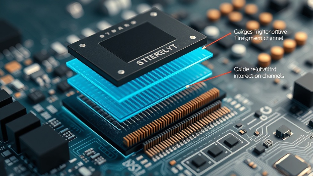
The core innovation lies in the integration of OSCs within a vertically stacked, monolithic 3D-DRAM structure. Traditional DRAM cells, typically composed of a capacitor and a transistor, occupy significant horizontal space on a chip. Stacking these cells vertically, or in 3D, is a well-established method for increasing density. However, implementing this with standard silicon-based transistors presents challenges, particularly concerning thermal management and process integration. The use of oxide semiconductors, known for their high electron mobility and suitability for low-temperature processing, offers a compelling alternative. This approach allows for the fabrication of the memory cells directly on top of each other without the extreme thermal budgets that can degrade underlying layers in conventional silicon processes.
The research paper, titled “Optimization of 3D-DRAM Architecture with Oxide-Semiconductor Channel through Process and Device Simulation,” outlines an integrated framework developed by the research teams. This framework combines process emulation, TCAD (Technology Computer-Aided Design) device simulation, parasitic extraction, and analytical modeling. Such a comprehensive approach is essential for understanding and optimizing the complex interplay of material properties, fabrication processes, and device behavior in this new architecture. By simulating these factors, the researchers can predict and refine the performance characteristics of the OSC-based 3D-DRAM cells before committing to expensive experimental fabrication.
Technical Approach and Simulation Framework
The investigation into the OSC-based 3D-DRAM architecture is underpinned by a sophisticated simulation methodology. The researchers employed process emulation to model the deposition, etching, and other critical fabrication steps involved in creating the stacked OSC layers and their associated circuitry. This is coupled with TCAD device simulation, which allows for the detailed analysis of electrical behavior at the transistor level. By simulating current flow, voltage characteristics, and potential leakage paths, the team can identify performance bottlenecks and areas for improvement.
Parasitic extraction plays a crucial role in accurately modeling the real-world performance of the memory cells. In highly integrated circuits, unintended electrical couplings between adjacent components (parasitics) can significantly degrade signal integrity and speed. The simulation framework accounts for these parasitic effects, providing a more realistic prediction of the DRAM's operational capabilities. Finally, analytical modeling is used to develop simplified mathematical representations of the device physics, enabling faster calculations and a deeper understanding of the fundamental scaling limits and performance trade-offs.
This integrated simulation approach is more than just a tool; it represents a paradigm shift in how complex memory architectures are designed and optimized. It allows for rapid iteration and exploration of design spaces that would be prohibitively time-consuming and costly with physical prototyping alone. The ability to simulate the entire process from material deposition to final device performance provides a holistic view, enabling researchers to make informed decisions about material selection, process parameters, and device geometry.
Potential Benefits and Future Implications
The successful development of a monolithic 3D-DRAM architecture using oxide semiconductors holds immense potential. Firstly, it offers a pathway to significantly higher memory densities compared to current planar or even conventionally stacked 3D-NAND flash memory. This is critical for meeting the storage and performance demands of next-generation data centers, mobile devices, and high-performance computing systems. The vertical integration minimizes the chip's footprint, allowing for more functionality within the same area or smaller overall form factors.
Secondly, OSCs are known for their excellent switching characteristics, including sharp subthreshold slopes. This means they can transition from an off-state to an on-state with a smaller change in gate voltage, leading to lower power consumption during operation. For battery-powered devices and large-scale data centers, this power efficiency translates directly into reduced operational costs and extended battery life.
The monolithic nature of the proposed 3D-DRAM is also a key advantage. It implies that the memory layers are fabricated in a single, continuous process flow, rather than being bonded or assembled from separate dies. This integrated fabrication can lead to shorter interconnects between memory cells and their control logic, reducing signal latency and further boosting performance. Shorter interconnects also mean reduced power loss due to resistance.
However, significant challenges remain. The reliability and endurance of OSCs in DRAM applications need to be thoroughly validated. While they offer advantages in certain aspects, their long-term stability under repeated read/write cycles and varying temperature conditions must meet the stringent requirements of memory products. Furthermore, scaling the fabrication processes to high-volume manufacturing levels will require close collaboration between research institutions and industry leaders like Samsung and Lam Research, who bring their extensive expertise in process technology and manufacturing.
What remains to be seen is how quickly this promising OSC-based 3D-DRAM architecture can transition from simulation and early research to tangible products. The path from a simulated architecture to a mass-produced memory chip is long and fraught with engineering hurdles. The successful demonstration of this technology could pave the way for a new era of ultra-dense, high-performance memory, fundamentally altering the landscape of semiconductor design and application.