JEDEC Unveils SPHBM4: A New Play in AI Memory Architecture
The Joint Electron Device Engineering Council (JEDEC), the body responsible for memory standards, has released the SPHBM4 specification. This new standard is poised to significantly impact the cost and performance of AI and high-performance computing systems by offering High Bandwidth Memory (HBM) class performance without the substantial expense of traditional silicon interposers and advanced packaging techniques like CoWoS (Chip-on-Wafer-on-Substrate). SPHBM4 aims to democratize access to high-bandwidth memory by enabling the use of more cost-effective organic substrates.
The Problem with Current AI Memory Solutions
Modern AI workloads, particularly those involving large language models and complex neural networks, demand immense memory bandwidth. High Bandwidth Memory (HBM), such as HBM2e and HBM3, has become the de facto standard for providing this, stacking DRAM dies vertically and connecting them to a processor via a silicon interposer. This interposer acts as a high-density wiring layer, allowing for a very wide data path (typically 1024 bits or more) between the stacked memory and the host processor.
However, the benefits of HBM come at a steep price. The manufacturing of silicon interposers is a complex and costly process, often requiring advanced lithography and wafer-level packaging. Furthermore, the integration of these components into advanced packaging solutions like CoWoS or advanced 2.5D/3D stacking adds further layers of expense and manufacturing complexity. For many AI applications, especially those deployed at scale or in cost-sensitive markets, these memory costs can become a prohibitive barrier, limiting the widespread adoption of the most powerful AI hardware.
SPHBM4's Approach: Narrow Interface, High Bandwidth
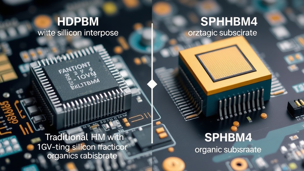
The core innovation of SPHBM4 lies in its architectural approach. Instead of relying on a wide, 1024-bit (or wider) interface that necessitates a silicon interposer for high density, SPHBM4 specifies a narrower, 512-bit interface. This might seem counterintuitive for a standard aiming for HBM-class bandwidth, but the key is how this narrower interface is implemented and what it enables.
By reducing the interface width, the physical routing density requirements on the substrate are significantly lessened. This allows for the use of organic substrates, which are considerably cheaper and easier to manufacture than silicon. Organic substrates are common in less demanding applications but have historically lacked the density and signal integrity to support the extreme bandwidth required by AI accelerators.
SPHBM4 achieves its goal by focusing on optimizing the signal transmission and interconnects within this 512-bit framework. While the exact technical specifications are detailed within the JEDEC standard, the implication is that through improved signaling techniques, tighter integration, and potentially higher clock speeds or more efficient data encoding, the bandwidth achievable over a 512-bit interface can rival that of wider, interposer-based solutions. This means that systems can achieve the necessary data throughput for AI tasks without the astronomical cost associated with silicon interposers and CoWoS-like packaging.
Implications for the AI Hardware Ecosystem
The release of SPHBM4 has far-reaching implications for the entire AI hardware ecosystem. For AI chip designers and system integrators, it offers a critical pathway to reduce the bill of materials (BOM) for their high-performance accelerators. This could lead to:
- Lower Cost AI Systems: By removing the need for expensive silicon interposers and CoWoS packaging, the overall cost of AI servers and specialized AI hardware can be dramatically reduced. This makes advanced AI capabilities more accessible to a broader range of businesses and researchers.
- Increased Design Flexibility: Organic substrates offer greater flexibility in terms of form factor and substrate size compared to silicon wafers. This could enable more diverse and specialized AI hardware designs.
- Improved Scalability: The reduced cost and complexity of SPHBM4-based memory solutions could accelerate the deployment of AI infrastructure, enabling greater scalability of AI model training and inference.
- New Market Opportunities: Companies specializing in organic substrate manufacturing, advanced packaging solutions for organic substrates, and memory controllers optimized for the SPHBM4 interface are likely to see new opportunities emerge.
The move towards a narrower interface for high bandwidth is a clever engineering trade-off. It acknowledges that the physical constraints and cost drivers of current advanced packaging solutions are becoming bottlenecks for AI deployment. SPHBM4 essentially provides a recipe for achieving the necessary performance without paying the premium for a silicon interposer. Think of it less like trying to fit a superhighway onto a tiny city block (which requires complex overpasses and underpasses) and more like optimizing a very efficient, multi-lane arterial road on a larger, more affordable piece of land.
What Nobody Has Addressed Yet: The Interoperability and Ecosystem Build-out
While SPHBM4 promises significant cost reductions, a critical question remains unanswered: how quickly and effectively will the ecosystem adopt and standardize this new interface? The success of any memory standard hinges not just on its technical merits but on the availability of compatible memory chips, controllers, and the willingness of major players to integrate it into their products. Will memory manufacturers readily produce SPHBM4-compliant DRAM? Will GPU and AI accelerator vendors pivot their designs to support this new interface, potentially fragmenting their product lines or requiring significant R&D investment? The transition from a widely adopted, albeit expensive, standard like HBM to a new, cost-optimized one like SPHBM4 is never instantaneous and will require significant coordination and investment across the industry. The speed at which this ecosystem matures will determine how quickly the promised cost savings materialize for end-users.
Looking Ahead: The Future of AI Memory
JEDEC's SPHBM4 standard represents a pragmatic and innovative step towards making advanced AI more affordable and accessible. By cleverly sidestepping the most expensive components of current high-bandwidth memory solutions, it opens the door for a new generation of cost-effective AI hardware. As AI continues its rapid proliferation across industries, solutions like SPHBM4 that address the fundamental cost drivers of compute and memory will be crucial in enabling its continued growth and widespread adoption.