Rethinking AI Memory: The High Cost of High Bandwidth Memory
High Bandwidth Memory (HBM) has become the de facto standard for accelerators powering AI and high-performance computing. Its stacked DRAM architecture, bonded to a GPU or CPU die via a silicon interposer, offers unparalleled memory bandwidth crucial for training and inference. However, this performance comes at a steep price. The silicon interposer itself is a complex, large, and expensive component, contributing significantly to the overall cost and packaging challenges of HBM-equipped processors. Furthermore, the manufacturing process for these large interposers, often requiring advanced nodes, introduces yield issues and limits scalability. As AI workloads continue to demand more memory capacity and bandwidth, the limitations and cost of traditional HBM are becoming increasingly apparent.
Intel's XBM: A Backend-Transistor Approach
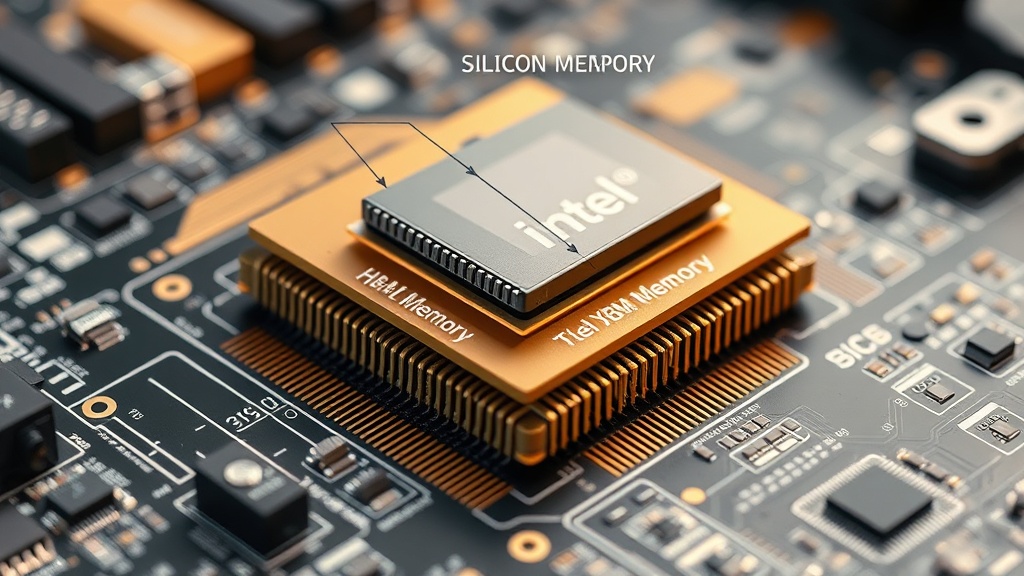
Intel's recently patented XBM (eXtreme Bandwidth Memory) architecture offers a potential paradigm shift. Instead of relying on a costly silicon interposer, XBM proposes a backend-transistor DRAM stack. This means the DRAM dies are stacked directly above the logic die (the GPU or CPU), with connections routed through the logic die's back-end-of-line (BEOL) metallization. This approach fundamentally changes the packaging requirements, potentially reducing complexity and cost. By integrating the memory stack more directly with the logic, XBM aims to achieve high bandwidth without the expensive intermediary silicon layer.
The core innovation lies in how the DRAM dies communicate with the logic. XBM leverages Universal Chiplet Interconnect Express (UCIe) links. UCIe is an open industry standard for chiplet-to-chiplet communication, designed for high-speed, low-latency, and low-power interconnects. Using UCIe allows for greater flexibility in combining different chiplets, including memory and logic, from various vendors or process nodes. This contrasts with the more monolithic and tightly integrated nature of traditional HBM, which is typically manufactured as a single package.
Integrated Repair Logic: A Critical Cost-Saver
One of the persistent challenges in stacking multiple DRAM dies, especially in advanced packaging techniques, is the increased probability of manufacturing defects. A single faulty die in a stack can render the entire memory module unusable, leading to significant yield losses. Intel's XBM patent addresses this head-on by incorporating built-in repair logic. This logic is designed to detect faulty DRAM dies within the stack and bypass them, effectively repairing the memory module without discarding the entire component.
This integrated repair capability is crucial for making the backend-transistor DRAM stack economically viable. By significantly improving yields, it lowers the cost per functional gigabyte of memory. Think of it less like trying to fix a broken circuit board after assembly, and more like having self-healing capabilities built into the fabric of the memory itself, allowing it to reroute around any minor imperfections. This proactive approach to defect management is vital for the mass production of complex, vertically integrated memory systems.
Implications for AI and Beyond
The potential benefits of Intel's XBM architecture are substantial, particularly for the memory-hungry AI sector. By eliminating the costly silicon interposer and employing a more cost-effective stacking method, XBM could lead to significantly cheaper high-performance memory solutions. This could make advanced AI accelerators more accessible and affordable, accelerating AI development and deployment across a wider range of applications and industries.
The use of UCIe links also promotes an open ecosystem. This could encourage broader industry adoption and innovation, allowing for greater customization and optimization of memory solutions tailored to specific workloads. Companies might be able to design custom memory stacks that precisely meet their bandwidth and capacity needs, rather than being locked into the fixed configurations of traditional HBM. This flexibility is a significant advantage in the rapidly evolving landscape of AI hardware.
While this is currently a patent filing, it signals Intel's strategic thinking about the future of memory technology. The company is exploring avenues to overcome the cost and complexity barriers that currently limit the scalability of high-performance memory. If XBM proves successful in development and manufacturing, it could represent a significant step forward in addressing the memory bottleneck that continues to challenge the full potential of artificial intelligence and other data-intensive computing domains.
The Unanswered Question of Performance
While the patent details a compelling architectural and cost-saving approach, the critical question remains: how will XBM's performance compare to established HBM standards? The patent outlines the potential for high bandwidth, but real-world benchmarks are needed to confirm if the UCIe links and backend-transistor routing can truly match or exceed the performance delivered by the tightly coupled, low-latency connections of HBM through its silicon interposer. The ultimate success of XBM will hinge on its ability to deliver both cost savings and competitive, or even superior, performance characteristics for the most demanding AI workloads.