
Intel Pioneers High-NA EUV in High-Volume Chip Production
Intel has achieved a significant milestone in semiconductor manufacturing, becoming the first company to ship high-volume logic chips produced using ASML's High Numerical Aperture (High-NA) Extreme Ultraviolet (EUV) lithography technology. This advancement means that select layers of Intel's upcoming Panther Lake processors, manufactured on the company's 18A process node, have been qualified and are now in production utilizing ASML's cutting-edge 0.55 NA EUV scanners. This marks a critical step forward in the relentless pursuit of smaller, more powerful, and more efficient integrated circuits.
The adoption of High-NA EUV is not merely an incremental upgrade; it represents a fundamental shift in lithography capabilities. Traditional EUV lithography, which uses a 0.33 NA optic, has been instrumental in enabling the transition to smaller process nodes. However, as feature sizes continue to shrink, the resolution limits of 0.33 NA EUV are being approached. High-NA EUV, with its higher numerical aperture of 0.55, can project finer patterns onto silicon wafers, allowing for the creation of even smaller transistors and more complex circuitry. This enhanced resolution is crucial for achieving the density and performance gains required for future generations of high-performance computing, AI accelerators, and mobile devices.
The specific application of High-NA EUV by Intel is on select layers of their Panther Lake processors. While the exact layers have not been disclosed, it is understood that these are critical for achieving the desired performance and power efficiency improvements that define the 18A process node. The 18A process node itself is a significant development for Intel, aiming to deliver substantial leaps in transistor density and performance over previous generations. Integrating High-NA EUV into the manufacturing flow for 18A is a testament to Intel's aggressive roadmap and its commitment to pushing the boundaries of what is technologically possible in chip fabrication.
The Significance of High-NA EUV
ASML's High-NA EUV system, known as the Twinscan EXE:5000, is a marvel of engineering. It uses a more complex optical system, including anamorphic optics, to achieve its higher NA. This allows it to print smaller features with greater precision. For context, think of it like upgrading from a standard magnifying glass to a high-powered microscope – you can now see and manipulate details that were previously invisible or impossible to work with. This increased resolution is essential for creating the next generation of logic chips that will power everything from advanced AI models to more sophisticated consumer electronics.
The move to High-NA EUV is not without its challenges. The machines are incredibly complex, large, and expensive, costing upwards of $350 million each. Furthermore, the transition requires significant adjustments to the entire manufacturing process, including mask design, wafer handling, and metrology. Intel's successful qualification and high-volume production using this technology underscore their deep expertise in advanced lithography and their strong partnership with ASML. This achievement is a clear signal that the industry is moving beyond the capabilities of current EUV and is embracing the next era of semiconductor manufacturing.
For Intel, this adoption is a strategic imperative. As the company strives to regain its leadership in process technology, mastering advanced lithography techniques like High-NA EUV is paramount. It allows them to compete more effectively with foundries like TSMC, which have historically led in process node advancements. By being the first to implement High-NA EUV in high-volume production, Intel demonstrates its technical prowess and its ability to execute on ambitious manufacturing roadmaps.
Panther Lake and the 18A Process Node
Panther Lake is the codename for Intel's next-generation client processor architecture, expected to succeed Lunar Lake and Arrow Lake. Processors built on the 18A node are anticipated to offer significant performance and efficiency improvements, making them competitive in the premium laptop and desktop segments. The integration of High-NA EUV on select layers is a key enabler for these improvements, allowing for finer transistor gates and denser interconnects. This translates directly into chips that can perform more calculations per clock cycle, consume less power, or both.
The 18A process node itself represents a major leap for Intel. It is designed to offer a 10% improvement in speed and a 20% reduction in power consumption compared to the 20A node, according to Intel's own projections. The node utilizes new transistor architectures like RibbonFETs and new interconnect technologies like Regal. The successful implementation of High-NA EUV on critical layers of this node is crucial for realizing these ambitious targets. It allows for the patterning of features that are simply not possible with existing 0.33 NA EUV or older lithography techniques.
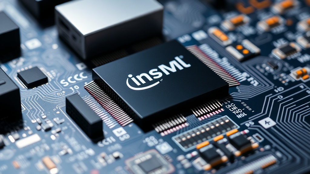
The dual qualification for 0.55 NA scanners means that Intel has validated the process on ASML's new generation of lithography equipment. This is a rigorous process that ensures the technology can be reliably used for mass production, meeting stringent yield and performance requirements. The fact that this qualification has been achieved for high-volume production so early in the technology's lifecycle is a remarkable feat and speaks to the collaborative efforts between Intel and ASML.
Broader Industry Implications
Intel's early adoption of High-NA EUV has several implications for the broader semiconductor industry. Firstly, it validates ASML's technology and accelerates its adoption timeline. Other foundries and Integrated Device Manufacturers (IDMs) will likely follow suit, although they may be dependent on the availability of these extremely complex and expensive machines. This move by Intel could put pressure on competitors to expedite their own High-NA EUV roadmaps.
Secondly, it signals a continued trend towards more advanced and specialized lithography techniques to overcome the physical limits of silicon. As Moore's Law continues to slow in its traditional form, innovation in manufacturing processes, including lithography, becomes increasingly critical for driving performance improvements. High-NA EUV is a key pillar in this ongoing effort. The ability to print ever-smaller features is essential for enabling the continued miniaturization and increased functionality of electronic devices, particularly in areas like artificial intelligence, high-performance computing, and advanced mobile processors.
What remains to be seen is the actual yield and performance uplift that Intel will achieve in its commercial products manufactured with High-NA EUV. While the technology promises finer features and better efficiency, translating these theoretical advantages into tangible benefits for end-users requires mastery of the entire manufacturing ecosystem. The success of Panther Lake and subsequent Intel chips will be a crucial benchmark for the industry's adoption of High-NA EUV.