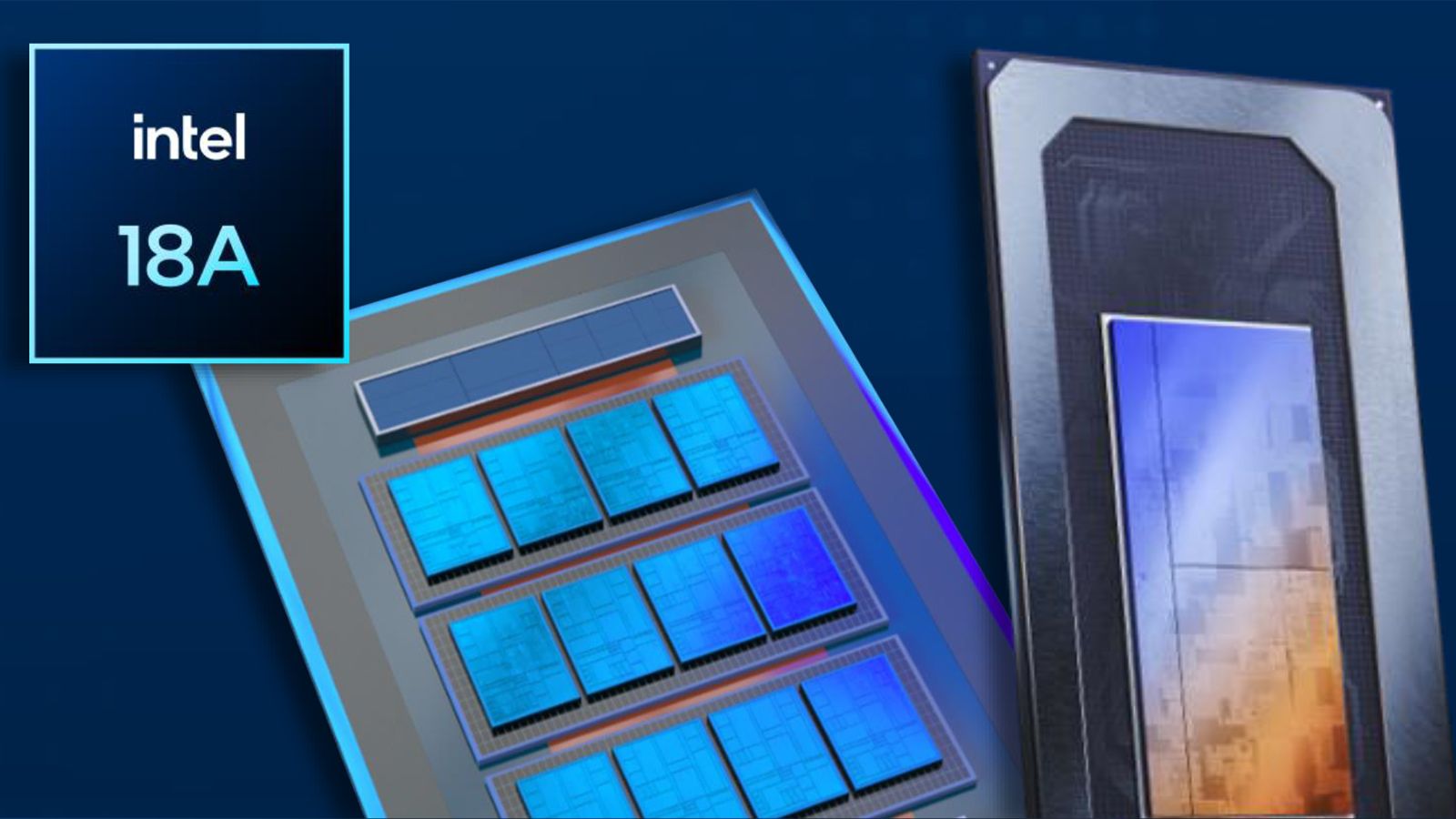
Intel's 18A Process Sees Significant Yield Improvements
Intel appears to have resolved critical wafer-to-wafer yield issues plaguing its advanced 18A process technology, according to recent reports. This marks a significant step forward for the chip giant as it aims to regain its manufacturing leadership. The improvements reportedly allow for production volumes of up to 15,000 wafers per month across both of Intel's key manufacturing sites.
The 18A process, a 1.8-nanometer class node, is central to Intel's aggressive 'IDM 2.0' strategy. This strategy not only aims to revitalize Intel's internal chip manufacturing but also positions the company as a foundry service provider for other chip designers. Overcoming yield challenges is paramount for any leading-edge semiconductor process, as it directly impacts cost, performance, and the ability to scale production to meet market demand.
Wafer-to-wafer (W2W) bonding is a complex manufacturing technique used in advanced packaging, particularly for chiplets. It involves aligning and fusing two or more wafers or dies with extreme precision, often with microscopic interconnects. For 18A, this process is crucial for enabling advanced 3D stacking and integration of heterogeneous components, a key differentiator for Intel's next-generation processors and those it plans to manufacture for external customers.
Early reports and industry speculation had highlighted W2W yield as a potential bottleneck for Intel's 18A roadmap. Low yields in such a sophisticated process translate directly into higher manufacturing costs per functional chip. For a foundry business model to be competitive, especially against established players like TSMC, achieving high yields at competitive price points is non-negotiable. The reported fix suggests Intel's engineering teams have made substantial progress in refining the alignment, bonding, and subsequent processing steps required for W2W integration at the 18A scale.
Production Capacity Boost
The claim of production reaching 15,000 wafers per month at both of Intel's primary fabrication facilities signifies a substantial ramp-up. This level of output is critical for Intel to not only supply its own upcoming products, such as the Lunar Lake and Panther Lake processors, but also to attract and service external foundry clients. For Intel Foundry Services (IFS) to be a credible alternative to existing foundries, it needs to demonstrate both technological capability and manufacturing scale.
Achieving 15,000 wafers per month for an entirely new, leading-edge process technology is an ambitious target. It implies that the fundamental process steps are stable and that the complex lithography, deposition, etching, and, crucially, the W2W bonding steps are performing reliably. This increased capacity also suggests that Intel is moving closer to mass production readiness for chips utilizing the 18A node.
The implications for Intel's competitive positioning are significant. By tackling and reportedly solving the W2W yield issues, Intel addresses a primary concern that could have delayed its roadmap or hampered its foundry ambitions. This progress could enable Intel to compete more effectively with TSMC and Samsung Foundry, which are also pushing the boundaries of semiconductor manufacturing with their own next-generation process nodes.
Broader Context and Future Outlook
While the resolution of W2W yield issues is a major positive development, it is important to acknowledge that other challenges may persist. Advanced semiconductor manufacturing is a multi-faceted endeavor, and a process node involves hundreds of individual steps, each with its own potential for defects and yield impact. Intel's 'Foveros' advanced packaging technology, which heavily relies on W2W bonding, is a key pillar of its product strategy, enabling the creation of complex, high-performance processors through the integration of smaller, specialized chiplets.
The success of 18A is not just about Intel's internal chip production; it's a crucial test for its foundry ambitions. Attracting third-party customers requires demonstrating not only leading-edge technology but also reliability, scalability, and cost-effectiveness. If these yield improvements are indeed validated, it significantly strengthens Intel Foundry Services' value proposition. Customers are looking for a viable, high-volume alternative to existing foundries, and Intel's ability to deliver on 18A is a key factor in that equation.
The timeline for widespread adoption of 18A in high-volume products remains a subject of intense scrutiny. However, the reported fix and production ramp suggest that Intel is on a path to meeting its internal targets and, potentially, its commitments to foundry customers. The industry will be watching closely as Intel moves from reported fixes to validated, high-volume production, and as its first 18A-manufactured products begin to reach the market.