The Evolving Landscape of Advanced Packaging
The semiconductor industry's relentless pursuit of smaller, faster, and more powerful chips has driven a significant shift towards advanced packaging technologies. Among these, Fan-Out Panel (FOP) packaging has emerged as a critical enabler for high-density interconnects and heterogeneous integration. This technology moves beyond traditional wafer-level packaging, utilizing larger panel substrates to accommodate multiple chiplets and increased routing density. However, this scaling introduces a host of new challenges for manufacturing processes, particularly in the realms of inspection and metrology. As feature sizes shrink and substrate warpage becomes more pronounced, existing inspection and metrology methods are being pushed to their limits. The ability to accurately and reliably inspect these complex structures is paramount to ensuring yield and performance.
Challenges in High-Density FOP Packaging
High-density fan-out panel packaging presents several formidable obstacles for inspection and metrology systems. One of the most significant is substrate warpage. Unlike rigid wafers, larger panels are more susceptible to bending and distortion during manufacturing processes. This warpage can vary across the panel, making it difficult to maintain consistent focus and alignment for optical inspection systems. Any deviation from a flat plane can lead to misinterpretations of feature dimensions, false positives for defects, or missed critical flaws. The increased routing density, characterized by finer Redistribution Layer (RDL) pitches and narrower trace sizes, further exacerbates this problem. Traditional inspection tools designed for coarser features struggle to resolve these minute details. Detecting defects like shorts, opens, or voids in RDLs with pitches below 10 micrometers requires vastly improved resolution and sensitivity. Furthermore, the complex 3D structures inherent in fan-out packaging, with multiple layers of RDLs and dielectric materials, demand metrology that can accurately measure layer thickness, uniformity, and alignment in three dimensions, not just on a 2D surface.
Advancements in Optical Inspection
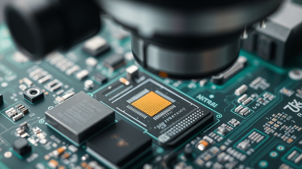
To address these challenges, significant advancements are being made in optical inspection methods. Machine vision systems are being equipped with higher-resolution cameras and more sophisticated lighting techniques to capture finer details. Techniques like confocal microscopy and phase-shifting interferometry are being adapted to overcome the focus issues caused by warpage, allowing for accurate measurements even on non-planar surfaces. Advanced algorithms are also being developed to compensate for substrate deformation in real-time. For RDL inspection, techniques such as dark-field illumination and structured light are proving effective in highlighting subtle defects like copper voids or over-etching that might be invisible under standard lighting. The goal is to move from purely visual defect detection to quantitative analysis of defect severity and impact. This involves not just identifying a defect but also measuring its dimensions and assessing its potential to cause functional failure. The development of AI and machine learning algorithms is also playing a crucial role, enabling systems to learn from vast datasets of images, identify new defect types, and improve detection accuracy over time.
Metrology for 3D Structures and Material Properties
Beyond surface inspection, metrology is critical for characterizing the 3D architecture of FOP packages. Techniques like Coherent Anti-Stokes Raman Scattering (CARS) microscopy are being explored for non-destructive, high-resolution imaging of dielectric materials and their properties within the package structure. X-ray computed tomography (XCT) is essential for inspecting the internal interconnects, bumps, and underfill materials, providing cross-sectional views without physically damaging the device. Advances in XCT technology are enabling faster scan times and higher resolution, making it more viable for in-line process control. Furthermore, metrology for material properties, such as the adhesion strength between different layers or the dielectric constant of insulating materials, is becoming increasingly important. Techniques like nanoindentation and electrical characterization are being integrated into the process flow to ensure the reliability and performance of the final package. The challenge lies in integrating these diverse metrology techniques into a seamless and efficient workflow that can keep pace with high-volume manufacturing demands.
The Role of In-line Metrology and Process Control
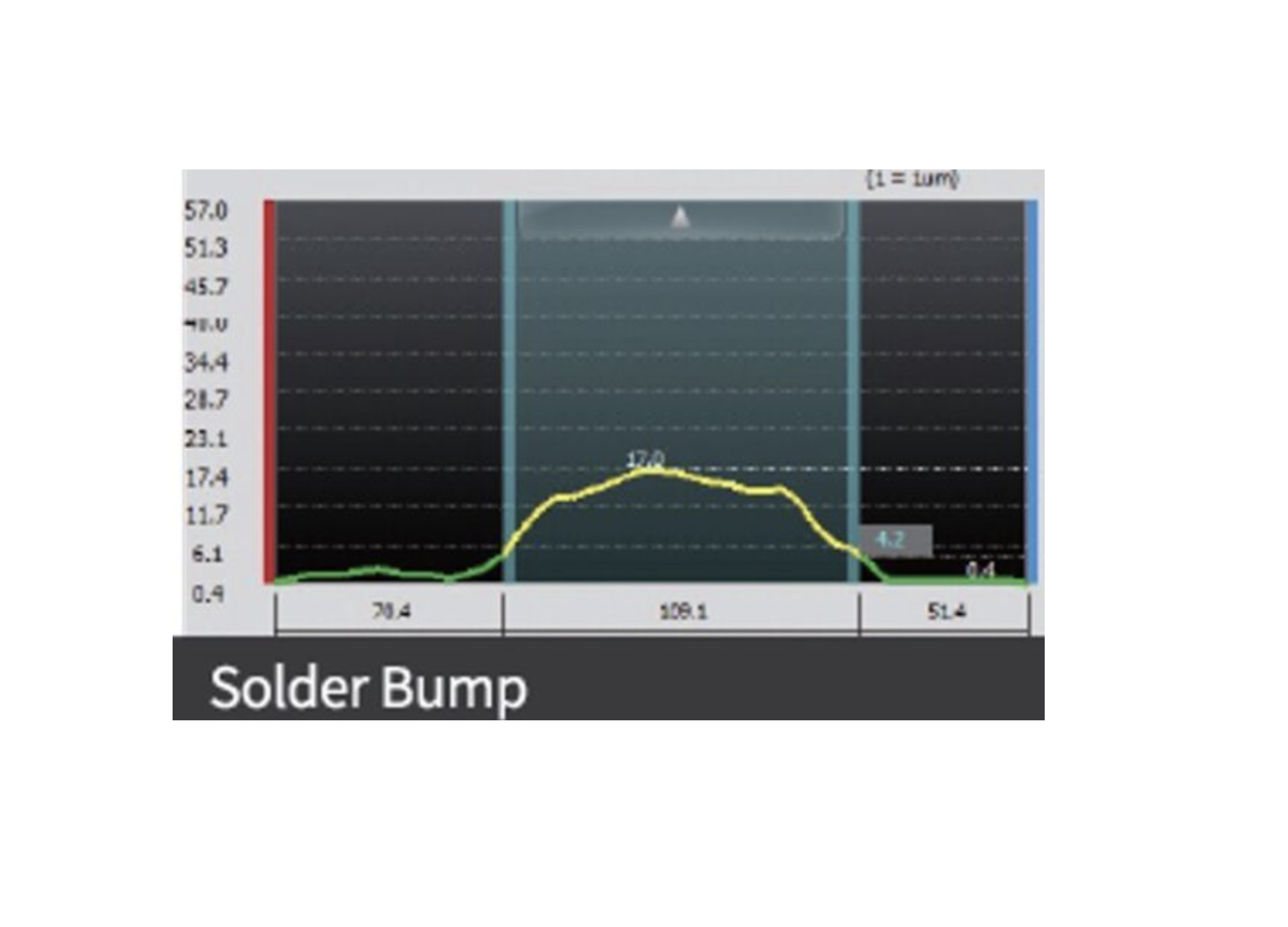
The ultimate goal is to shift from end-of-line testing to in-line metrology and process control. By gathering data at multiple stages of the manufacturing process, manufacturers can identify and correct issues as they arise, rather than discovering them only after significant investment in downstream processing. This requires metrology tools that are not only accurate but also fast and robust enough to operate in a production environment. Automated optical inspection (AOI) systems are becoming more integrated with process equipment, allowing for immediate feedback loops. For example, if an AOI system detects excessive RDL pitch variation after a lithography step, the system can automatically adjust parameters for the next lithography exposure or flag the panel for rework before further processing. Similarly, in-line XCT can verify the quality of solder bumps before die attach, preventing costly failures later. This proactive approach to quality control is essential for achieving high yields in the complex and sensitive FOP manufacturing process. The integration of data analytics and machine learning further enhances this capability, enabling predictive maintenance of equipment and optimization of process recipes based on real-time metrology data.
Future Directions and Industry Collaboration
The ongoing evolution of fan-out panel packaging, particularly towards even higher densities and novel materials, will continue to push the boundaries of inspection and metrology. Future developments are likely to focus on further miniaturization of inspection probes, enhanced sensitivity to subtle defects, and improved 3D metrology capabilities. The industry recognizes that no single technology will solve all challenges. Therefore, collaboration between equipment manufacturers, semiconductor foundries, and materials suppliers is crucial. Standards for defect classification and performance metrics will be necessary to ensure interoperability and comparability across different systems. The development of digital twins and advanced simulation tools will also play a role, allowing for virtual testing and optimization of inspection strategies before physical implementation. As FOP packaging becomes more pervasive, the sophistication of the tools used to ensure its quality will need to advance in lockstep, transforming manufacturing floors into highly monitored and controlled environments.