HBM's Complexity Demands New Assembly Approaches
High-bandwidth memory (HBM) is no longer just a niche component for high-performance computing. Its intricate design, involving multiple memory dies stacked vertically and interconnected via through-silicon vias (TSVs), presents significant challenges for semiconductor manufacturers. This complexity, however, is also acting as a powerful catalyst for innovation in 3D assembly, testing, and reliability methodologies. The stringent requirements for performance, power efficiency, and signal integrity in HBM are pushing the boundaries of what was previously possible in wafer-level and die-level packaging.
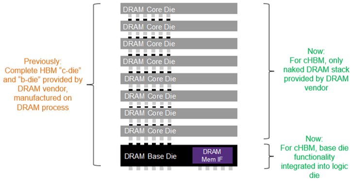
The fundamental challenge with HBM lies in its three-dimensional nature. Unlike traditional 2D integrated circuits, HBM stacks DRAM dies on top of each other, often with a logic interposer or base die at the bottom. These dies are connected using TSVs, which are vertical electrical connections passing through the silicon substrate. The sheer number of TSVs, the precision required for their alignment, and the thermal management across multiple stacked layers create a complex manufacturing process. Achieving high yield in such a stacked architecture is exponentially harder than in planar designs. Each layer added increases the potential for defects, and a single faulty die or TSV connection can render the entire stack unusable.
This escalating complexity has made HBM a critical testbed for advanced 3D assembly techniques. Manufacturers are investing heavily in developing new processes for die bonding, interposer fabrication, and TSV integration that can achieve higher throughput and better yields. Techniques like micro-bumps, hybrid bonding, and advanced wafer-level packaging are being refined and scaled specifically to meet the demands of HBM production. The success or failure of these techniques in HBM directly influences their adoption in other advanced packaging technologies, making HBM a bellwether for the future of 3D semiconductor manufacturing.
The Role of Design for Testability (DFT)
The intricate nature of 3D stacked HBM makes traditional testing methods insufficient. Ensuring that every memory die, every TSV, and every connection between them functions correctly requires a sophisticated approach to Design for Testability (DFT). DFT strategies are being adapted and enhanced to specifically address the challenges posed by vertically integrated structures. This includes developing new scan architectures, built-in self-test (BIST) mechanisms, and at-speed testing methodologies capable of probing the performance of the entire stack under realistic operating conditions.
One of the key DFT challenges in HBM is testing the TSVs themselves. A faulty TSV can lead to intermittent failures or complete loss of connectivity. Advanced DFT techniques aim to isolate and test individual TSVs or groups of TSVs to identify defects early in the manufacturing process. This often involves specialized test patterns and access methods that can probe these vertical connections without compromising the overall die integrity. Furthermore, the high-speed interfaces and the sheer volume of data processed by HBM necessitate at-speed testing, which requires test equipment capable of operating at the memory's native frequencies.
The integration of logic and memory in HBM also complicates DFT. The logic die, which manages the memory access, must be tested in conjunction with the stacked DRAM dies. This requires a holistic DFT strategy that accounts for the interactions between different components within the package. The goal is to achieve comprehensive test coverage while minimizing test time and cost, a delicate balancing act given the complexity of the HBM architecture. The lessons learned from implementing DFT for HBM are directly informing the development of test strategies for future heterogeneous integration and 3D ICs.
Ensuring Reliability in Stacked Architectures
Beyond initial functionality, the long-term reliability of HBM is paramount, especially given its use in critical applications like AI accelerators and high-performance servers. The stacked nature of HBM introduces unique reliability concerns that differ significantly from planar designs. Thermal management, mechanical stress, and the long-term stability of TSVs and interconnections are all critical factors that must be addressed.
Thermal management is a significant hurdle. With multiple dies stacked closely together, heat generated by one layer can impact the performance and longevity of the layers above and below it. Advanced thermal interface materials (TIMs), sophisticated cooling solutions, and optimized power delivery networks are essential to prevent thermal runaway and ensure stable operation. The reliability of these thermal solutions is itself a subject of intense research and development.
Mechanical reliability is another area of focus. The bonding processes used to stack dies, the interposer, and the substrate can introduce stresses. These stresses can be exacerbated by temperature cycling during operation and manufacturing. Ensuring that the interconnections, particularly the TSVs and micro-bumps, can withstand these stresses over the product's lifespan is critical. Accelerated stress testing, including temperature cycling, humidity testing, and burn-in, are employed to identify potential failure mechanisms and validate the robustness of the HBM design and assembly process. The insights gained from HBM reliability testing are invaluable for predicting and mitigating failure modes in other advanced 3D packaging technologies.
The Path Forward: Yield Optimization and Future Applications
The continuous drive to improve yield in HBM manufacturing is not just about cost reduction; it's about enabling the wider adoption of HBM technology and paving the way for even more complex future architectures. As HBM evolves into HBM3 and beyond, the number of stacked dies and the density of TSVs are expected to increase, further intensifying the challenges for assembly and testing. Manufacturers are exploring new materials, advanced metrology, and AI-driven process control to achieve higher yields.
The advancements spurred by HBM are not confined to memory. The techniques developed for 3D assembly, DFT, and reliability are transferable to other heterogeneous integration platforms. This includes chiplets, advanced logic-die stacking, and integrated photonic devices. Essentially, HBM is serving as a high-stakes playground where the semiconductor industry is learning to master the art of building upwards, a skill that will be crucial for the continued scaling of computing performance.
If you are developing systems that rely on cutting-edge AI accelerators or high-performance computing infrastructure, the progress in HBM yield directly impacts the availability, performance, and cost of these critical components. The ability to reliably stack more memory and integrate it tightly with processing units is fundamental to the next generation of computational power. The ongoing innovation in HBM assembly and testing ensures that these demanding applications will have the memory bandwidth they require.