The Promise and Peril of Fine-Pitch Hybrid Bonding
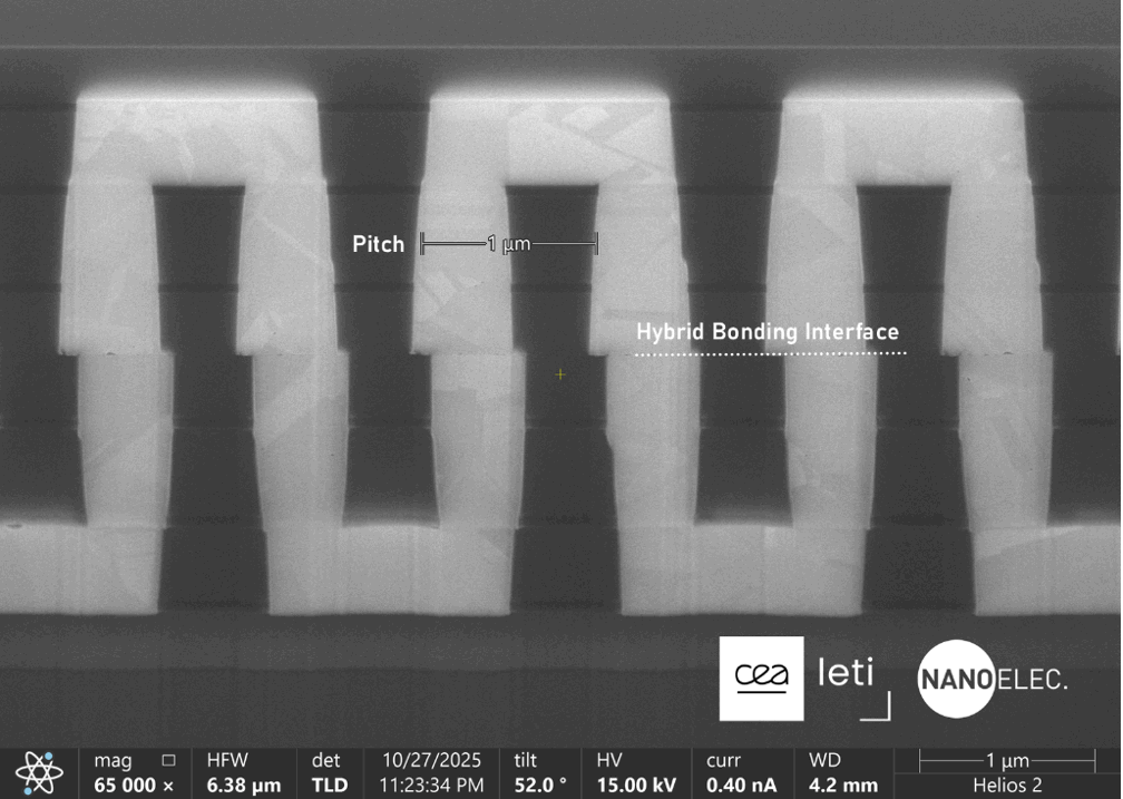
Hybrid bonding, a technique that directly connects dies or wafers without solder bumps, promises denser interconnects and improved performance. While already in production for certain applications, the push towards finer pitches—essential for advanced packaging like 3D integration—introduces substantial manufacturing complexities. The core challenge lies in scaling these advanced interconnects to the high volumes and cost points demanded by the semiconductor industry, a transition that requires maintaining exquisite control over wafer surfaces and alignment throughout the back-end manufacturing process.
Current hybrid bonding implementations, often used in stacked image sensors or DRAM, typically operate at pitches around 10-20 micrometers. The ambition is to shrink these pitches to 5 micrometers and below, enabling significantly higher interconnect densities. This miniaturization, however, amplifies the sensitivity to any imperfections on the bonding surfaces. Even nanoscale variations can lead to bonding failures, dramatically impacting yield. Achieving die-to-wafer or wafer-to-wafer integration at these fine pitches necessitates a level of precision that pushes the boundaries of current fab capabilities.
The semiconductor industry operates on rigorous yield targets and cost structures. For hybrid bonding to transition from niche applications to mainstream, high-volume manufacturing (HVM), it must align with the throughput and economic models of established backend processes. This means not only achieving reliable bonding but doing so at speeds comparable to traditional methods, with minimal additional cost. The delicate nature of the direct copper-to-copper or dielectric-to-dielectric interfaces at sub-5-micron pitches means that any contamination, particle, or surface deformation can be catastrophic. This demands unprecedented levels of cleanliness and precision in handling, metrology, and the bonding process itself.
Surface Control: The Unseen Battleground
The success of hybrid bonding hinges on creating atomically smooth, pristine surfaces on both bonding partners. In fine-pitch applications, even a few nanometers of surface roughness or a single sub-micron particle can prevent the formation of a reliable bond. This is particularly true for the direct metal-to-metal (copper-to-copper) or dielectric-to-dielectric interfaces that are characteristic of hybrid bonding. Unlike traditional flip-chip bonding, which relies on solder bumps that can tolerate some surface imperfections and provide a stand-off, hybrid bonding requires intimate contact.
Achieving this level of surface perfection at scale involves multiple stages. First, advanced CMP (Chemical Mechanical Planarization) processes are needed to ensure the wafer surfaces are atomically flat. Following CMP, wafer cleaning becomes paramount. Traditional cleaning methods may not be sufficient to remove all residues or nanoparticles without damaging the sensitive dielectric layers or metal interconnects. New, gentler, yet highly effective cleaning chemistries and processes are under development. Furthermore, the passivation layer, often an oxide or nitride, must be perfectly formed and free of defects to ensure uniform dielectric properties across the entire wafer.
The challenge is compounded by the need to maintain these pristine surfaces throughout the manufacturing flow. Exposure to the environment, handling by robotic arms, and subsequent processing steps all present opportunities for contamination. This necessitates a highly controlled cleanroom environment, advanced wafer handling techniques, and potentially in-situ metrology to verify surface integrity immediately before bonding. The cost associated with achieving and maintaining such stringent control across millions of wafers is a significant hurdle for HVM.
Alignment Precision: A Nanometer-Scale Dance
Beyond surface preparation, the alignment of dies or wafers during the bonding process is critical. For fine-pitch interconnects, the alignment tolerance shrinks dramatically. A 5-micron pitch requires alignment accuracy in the sub-micron range, often down to tens of nanometers. This level of precision must be achieved consistently across the entire wafer, even when bonding dies from different wafers or from different process lots.
Current alignment systems, while sophisticated, are designed for larger features and greater tolerances. Scaling these systems to nanometer-level accuracy for high-volume throughput requires significant advancements. Factors such as thermal expansion, vibration, and mechanical stability of the bonding equipment become major concerns. The bonding tools themselves must be engineered with extreme precision, incorporating advanced optical metrology for real-time alignment correction.
The complexity is further amplified in die-to-wafer bonding, where individual dies are picked from a donor wafer and placed onto a receiver wafer. This process involves complex pick-and-place mechanics, precise die orientation, and accurate placement relative to the wafer's existing circuitry. If the dies are not perfectly aligned, the fine-pitch interconnects will misalign, leading to short circuits or open circuits. The yield loss from even a small percentage of misaligned dies can render the entire process economically unviable for HVM.
Exploring Alternative Materials for Enhanced Bonding
To address some of the challenges associated with purely copper-to-copper or dielectric-to-dielectric bonding, researchers are exploring alternative materials and approaches. These materials aim to improve bonding robustness, reduce the sensitivity to surface imperfections, or enable lower bonding temperatures and pressures.
One promising area is the use of nanotwinned copper. This material exhibits enhanced mechanical properties and can potentially facilitate more reliable interdiffusion at the bonding interface, even with slight surface variations. Another avenue involves novel dielectric materials like SiCN (Silicon Carbon Nitride), which can offer improved mechanical strength and thermal stability compared to traditional oxides. BCB (Benzocyclobutene), a polymer dielectric, is also being investigated for its potential to act as a compliant layer, absorbing some of the surface roughness and stress during bonding.
Furthermore, the use of passivating metals is being explored. These ultra-thin metal layers, deposited on top of the copper or dielectric, can act as a sacrificial layer that promotes wetting and bonding while protecting the underlying material. The precise composition and deposition of these passivating layers are critical to ensure they do not impede electrical conductivity or introduce new failure mechanisms. The development and qualification of these alternative materials add another layer of complexity to the path towards HVM, requiring new process integration and reliability testing.
The Path Forward: Integration and Metrology
The transition of fine-pitch hybrid bonding to high volume is not solely a materials or equipment challenge; it is an integration challenge. It requires a holistic approach that considers the entire manufacturing flow, from wafer fabrication to final packaging. This includes developing robust metrology solutions capable of inspecting and verifying bond quality at the nanoscale, both before and after bonding.
Advanced inline metrology, such as atomic force microscopy (AFM) or advanced optical inspection techniques, will be crucial for monitoring surface flatness, particle contamination, and alignment accuracy in real-time. Developing predictive models based on this data can help identify potential bonding issues early in the process, allowing for corrective actions and minimizing scrap. The cost of implementing such comprehensive metrology across a high-volume fab is substantial, but essential for achieving acceptable yields.
Ultimately, the success of fine-pitch hybrid bonding in HVM will depend on a concerted effort from material suppliers, equipment manufacturers, and chipmakers. Significant investment in R&D, process optimization, and new manufacturing infrastructure will be required. If these challenges can be met, the reward is a pathway to unprecedented device density and performance, enabling the next generation of advanced electronic systems.