The Escalating Complexity of Semiconductor Process Engineering
The semiconductor industry is locked in a perpetual race for miniaturization and performance enhancement. This relentless drive, however, introduces unprecedented complexity into the process engineering workflows that underpin chip manufacturing. As feature scales shrink to nanometer levels, the interplay of physics, materials science, and manufacturing variables becomes exponentially more intricate. Traditional simulation methods, while powerful for isolated tasks, often struggle to capture the holistic, dynamic nature of these advanced processes. Process engineers find themselves navigating a rapidly expanding innovation space, demanding tools that can not only predict outcomes but also provide actionable insights into the underlying mechanisms and potential interactions.
This growing complexity means that a change in one process step can have cascading, often unpredictable, effects on subsequent steps and the final device performance. Engineers need to explore, understand, and act on this interconnectedness with greater precision and speed than ever before. The challenge lies in moving beyond static, feature-scale simulations that analyze individual aspects of the fabrication process in isolation. What is required are dynamic, integrated environments that mirror the real-world manufacturing flow, allowing for comprehensive analysis and optimization.
From Feature-Scale Simulation to Digital Twins
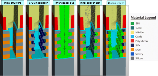
The evolution from traditional feature-scale simulation to the concept of digital twins represents a significant leap forward for process engineering. Feature-scale simulations typically focus on the physics governing a specific device feature, such as etching a gate or depositing a dielectric layer. These simulations are critical for understanding the fundamental science at play and for optimizing localized parameters. However, they often operate within a simplified context, neglecting the broader manufacturing environment and the cumulative impact of preceding and succeeding steps.
Digital twins, in contrast, are dynamic virtual replicas of a physical process or system. For semiconductor process engineering, this means creating a comprehensive virtual model that encompasses not just individual process steps but also their sequence, interdependencies, and the flow of materials through the fab. These twins are built on physics-grounded workflows, meaning they leverage fundamental physical laws and models to ensure accuracy. Crucially, they are designed to be continuously updated with real-time or near-real-time data from the physical manufacturing line, allowing them to accurately reflect the current state of the process.
The Power of Physics-Grounded Workflows
The efficacy of digital twins hinges on their foundation in physics. Unlike purely data-driven models that might identify correlations, physics-grounded workflows ensure that the simulations are rooted in the fundamental scientific principles that govern semiconductor fabrication. This allows engineers to trust the predictions and to gain a deeper understanding of the ‘why’ behind observed phenomena. For instance, simulating plasma etching requires accurate models of fluid dynamics, chemical kinetics, and electromagnetic fields. A physics-grounded approach ensures these elements are modeled correctly, providing reliable insights into etch profiles, selectivity, and uniformity.
These workflows enable process teams to perform a wide range of critical tasks. They can explore the impact of novel materials or process variations in a risk-free virtual environment before committing to expensive experimental runs. They can diagnose yield excursions or performance deviations by tracing the issue back through the digital twin, identifying the most probable root causes. Furthermore, they can proactively optimize process parameters to achieve desired outcomes, such as improving wafer-to-wafer consistency or reducing process variability. This predictive and diagnostic capability is essential for staying ahead in an industry characterized by rapid innovation and intense competition.
Navigating the Expanding Innovation Space
The semiconductor innovation space is expanding not only in terms of feature complexity but also in the sheer number of potential design and process permutations. Advanced packaging techniques, heterogeneous integration, and novel materials all add layers of complexity that traditional methods struggle to manage. Digital twins offer a framework to systematically explore this vast landscape. By providing a unified, dynamic view of the entire manufacturing process, they enable engineers to test hypotheses, evaluate trade-offs, and identify optimal pathways more efficiently.
Consider the challenge of integrating new materials. A digital twin can model how a new dielectric material will behave during deposition, etching, and planarization, and critically, how it will interact with neighboring materials and device structures throughout the entire fabrication sequence. This holistic view prevents the unintended consequences that often arise when optimizing a single step in isolation. It allows for a more informed and integrated approach to innovation, reducing the time and cost associated with bringing new technologies to market.
The Future: Predictive Maintenance and Autonomous Control
The ultimate aspiration for digital twins in process engineering is to move towards predictive maintenance and, eventually, autonomous process control. By continuously monitoring the virtual replica against the physical reality, deviations can be detected long before they lead to significant yield loss or quality issues. This allows for proactive adjustments to be made, preventing problems before they occur. The data generated and the insights gained from the digital twin can also inform the development of more sophisticated control algorithms.
While fully autonomous fabs are still some way off, digital twins are laying the groundwork. They provide the necessary understanding of process dynamics and the ability to predict outcomes under various conditions. This information is crucial for developing intelligent systems that can adapt to changing conditions, optimize performance in real-time, and ensure the highest levels of quality and efficiency. The journey from feature-scale simulation to comprehensive digital twins is not just an incremental improvement; it is a fundamental shift in how process engineers will design, monitor, and optimize the complex manufacturing processes that define the future of electronics.