
Near-Memory HBM for Large Language Model Inference
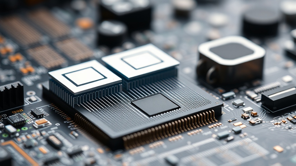
The escalating demands of large language models (LLMs) for memory bandwidth and capacity are driving innovation in semiconductor architecture. A key area of focus is High Bandwidth Memory (HBM), particularly its application in near-memory processing for LLM inference. Researchers are exploring how HBM can be integrated more closely with processing units to reduce data movement, a significant bottleneck in current AI hardware. This involves not only optimizing the HBM stacks themselves but also developing novel ways to process data directly within or adjacent to the memory, effectively bringing computation closer to the data.
The challenge with LLMs is their substantial memory footprint and the constant need to fetch vast amounts of parameters and intermediate states. Traditional architectures, even with advanced caches, struggle to keep pace. Near-memory HBM approaches aim to alleviate this by enabling higher data transfer rates and lower latency. This could involve placing compute logic directly on the HBM interposer or adjacent to the memory dies. The benefits are multifold: reduced power consumption due to less data movement, increased inference throughput, and potentially smaller form factors for AI accelerators. The papers in this domain often delve into the architectural trade-offs, such as the complexity of co-designing memory and compute, and the thermal implications of concentrating processing power near memory.
Processing-in-Memory for 3D DRAM and SDV Hardware Abstraction
Beyond HBM, the concept of processing-in-memory (PIM) is being investigated for other memory technologies, including 3D DRAM. PIM seeks to perform computations directly within the memory array, bypassing the conventional von Neumann bottleneck where data must shuttle between the CPU and memory. For 3D DRAM, this could unlock significant performance gains and energy efficiency improvements, especially for applications with high data parallelism. Researchers are looking at how to embed simple logic gates or specialized processing units within the 3D stacked DRAM structure itself, enabling basic operations like logical AND, OR, or even simple arithmetic to be executed in situ.
Concurrently, the automotive industry is pushing for standardization in hardware abstraction layers (HALs) for Software-Defined Vehicles (SDVs). This effort aims to create a more modular and flexible software architecture, allowing for easier updates, feature additions, and cross-platform compatibility. The technical papers in this area focus on defining common interfaces and protocols that abstract away the underlying hardware complexities, such as specific sensor interfaces, ECU communication protocols, and powertrain control units. The goal is to enable developers to write software once and deploy it across a wide range of vehicle platforms, accelerating innovation in automotive software and services.
Advanced Semiconductor Fabrication: GAAFETs, Lithography, and Material Science
The relentless pursuit of smaller, faster, and more power-efficient chips continues to drive advancements in fabrication processes. Papers discussing 3nm Gate-All-Around FETs (GAAFETs) are exploring critical issues such as self-heating effects and radiation hardness. GAAFETs, with their gate wrapping entirely around the channel, offer improved electrostatic control over traditional FinFETs, enabling further scaling. However, the increased device density and potential for hot carrier injection raise concerns about thermal management and reliability, particularly in demanding environments. Research here focuses on characterizing these effects and developing mitigation strategies, such as advanced thermal interface materials and optimized device structures.
The development of thin Transition Metal Dichalcogenide (TMD) transistors represents another frontier in materials science for semiconductors. TMDs offer unique electronic properties that could enable novel device architectures beyond silicon. Thin-film TMD transistors are being explored for their potential in flexible electronics, low-power logic, and advanced sensing applications. The challenges lie in reliably fabricating these thin films with consistent properties and integrating them into existing semiconductor manufacturing flows.
Furthermore, advancements in diamond defect detection are crucial for the burgeoning field of quantum computing and sensing. Diamond, with its nitrogen-vacancy (NV) centers, is a promising material for qubits and highly sensitive magnetometers. However, the presence and precise control of these defects are critical for performance. New techniques for detecting and characterizing diamond defects are essential for fabricating reliable quantum devices. Similarly, research into roll-to-roll lithography techniques aims to enable high-throughput, cost-effective manufacturing of advanced electronic components on flexible substrates, potentially revolutionizing the production of displays, sensors, and printed electronics.
Monolithic CMOS-Photonic Integration and AI in Thermal Modeling
The integration of photonics with CMOS technology on a single chip is a significant area of research, promising to enable high-speed optical communication and advanced sensing capabilities directly within standard semiconductor foundries. Monolithic CMOS-photonic integration aims to combine the strengths of electronic and photonic devices on a single substrate, reducing the cost and complexity associated with hybrid approaches. This is particularly relevant for data centers and high-performance computing, where optical interconnects are becoming essential for overcoming bandwidth limitations.
The complexity of thermal management in advanced 3D integrated circuits, especially those involving photonic components, is also a major concern. AI-driven thermal modeling is emerging as a powerful tool to predict and manage heat dissipation in these intricate structures. By leveraging machine learning algorithms, researchers can develop more accurate and efficient thermal models, enabling better design decisions and preventing overheating. This AI approach allows for faster simulation cycles and the optimization of thermal performance in ways that were previously intractable with traditional simulation methods.
Quantum Photonic Chips and the Future of Computing
Quantum photonic chips represent a distinct path toward scalable quantum computing. Unlike superconducting or trapped-ion approaches, photonic quantum computing leverages particles of light (photons) and optical components. Research in this area focuses on developing efficient single-photon sources, low-loss waveguides, and high-fidelity single-photon detectors, all integrated onto a single chip. The potential advantages include room-temperature operation (in some designs) and compatibility with existing silicon fabrication infrastructure, although challenges remain in achieving deterministic photon generation and robust entanglement operations.
The convergence of these diverse research threads—from memory architectures optimized for AI, to advanced materials and fabrication methods, to novel computing paradigms like photonics and quantum mechanics—underscores the dynamic and rapidly evolving nature of the semiconductor industry. Each paper, while addressing a specific technical challenge, contributes to the broader ecosystem of innovation that will define the next generation of computing hardware.