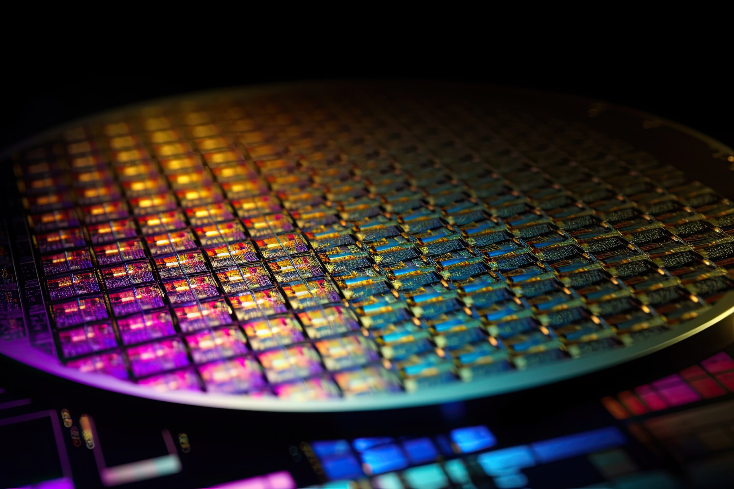
AI-Driven Semiconductor Property Prediction
Researchers are increasingly leveraging artificial intelligence to accelerate the discovery and optimization of semiconductor materials. A recent development, detailed in Semiconductor Engineering, showcases a neural network capable of predicting key semiconductor properties. This approach bypasses the need for extensive, time-consuming experimental trials, which are traditionally a bottleneck in material science research.
The neural network is trained on vast datasets of existing material properties and their corresponding structures. By learning the complex relationships between atomic composition, crystal structure, and electrical or optical characteristics, the AI can then predict the behavior of novel or untested materials. This predictive power is crucial for identifying candidate materials for next-generation electronic devices, such as faster transistors, more efficient solar cells, or advanced memory technologies.
Traditionally, the process of finding a new semiconductor material with specific desired properties involved a laborious cycle of synthesis, characterization, and testing. Each step could take weeks or months, and the search space of possible material combinations is astronomically large. AI models can sift through this space orders of magnitude faster, identifying promising avenues for experimental validation. This not only speeds up the R&D process but also reduces the cost associated with material exploration.
The implications for the semiconductor industry are profound. Faster material discovery means shorter design cycles for new chips, enabling quicker responses to market demands and technological shifts. It also opens doors to exploring materials previously deemed too difficult or expensive to investigate, potentially leading to breakthroughs in performance, power efficiency, and form factor for electronic devices.

Ferroelectric Titanium Dioxide Thin Films
Beyond AI-driven prediction, fundamental material science research continues to explore novel materials for specific applications. One such area of focus is ferroelectric titanium dioxide (TiO2) thin films. Ferroelectric materials possess a unique property: their electric polarization can be reversed by an external electric field. This characteristic makes them highly valuable for non-volatile memory, sensors, and energy harvesting devices.
Titanium dioxide, commonly known as titanium white, is an abundant and relatively inexpensive material. However, achieving stable and efficient ferroelectric properties in TiO2 thin films requires precise control over its crystalline structure and stoichiometry. Researchers are investigating various deposition techniques, such as atomic layer deposition (ALD) or pulsed laser deposition (PLD), to create these highly ordered thin films with tailored properties.
The challenge lies in overcoming the inherent paraelectric nature of bulk TiO2 and inducing ferroelectricity in thin film forms. This often involves doping the TiO2 with specific elements or creating specific crystal phases, such as the orthorhombic or monoclinic phases, which exhibit ferroelectric behavior, unlike the more common rutile and anatase phases. Understanding the relationship between film thickness, deposition conditions, doping concentration, and the resulting ferroelectric response is critical for practical device integration.
The successful development of reliable ferroelectric TiO2 thin films could lead to smaller, more energy-efficient memory components, such as ferroelectric RAM (FeRAM), which offers high speed and low power consumption. Furthermore, their potential in sensing applications, where changes in electric field can be detected, and in piezoelectric devices for energy harvesting, makes this an active area of research with significant technological promise.
Bidirectional Pixels for Enhanced Displays
The pursuit of better display technologies is another frontier where novel research is emerging. A concept for "bidirectional pixels" has been explored, aiming to improve the efficiency and performance of displays. Traditional pixels emit light in a single direction, typically outwards towards the viewer. Bidirectional pixels, however, are designed to control light emission in two opposing directions.
This dual-directionality could offer several advantages. For instance, a portion of the light that would normally be lost within the display stack could potentially be reflected back or redirected, increasing overall light usage efficiency. This could translate to brighter displays with lower power consumption, a critical factor for mobile devices and large-format screens.
The technical implementation of bidirectional pixels likely involves advanced optical engineering, potentially incorporating micro-lenses, reflective layers, or light-guiding structures within each pixel. The goal is to precisely manage the path of photons emitted by the display's light source, such as LEDs or micro-LEDs, or emitted by the light-emitting elements themselves, like in OLEDs.
Beyond efficiency, bidirectional control might also enable new display functionalities. This could include advanced stereoscopic 3D displays that require precise control of light paths, or even novel forms of augmented reality interfaces where light can be directed both towards the user and towards external sensors or cameras simultaneously. While still in the research phase, the concept of bidirectional pixels represents an innovative approach to pushing the boundaries of display technology.
These diverse research efforts – from AI-accelerated material discovery to fundamental explorations in ferroelectrics and novel optical designs for pixels – highlight the dynamic and multifaceted nature of innovation in semiconductor and display technologies. Each area holds the potential to unlock significant advancements in computing, energy, and consumer electronics.