The Limits of Conventional Process Monitoring
For decades, the semiconductor industry has relied on ring oscillators as a primary method for monitoring process variations in silicon wafers. These simple circuits, consisting of an odd number of inverters in a loop, generate a clock signal whose frequency is directly sensitive to the speed of the individual transistors. By measuring this frequency, engineers could infer changes in critical process parameters like threshold voltage (Vt) and gate length. However, this approach has significant limitations in today's complex, multi-parameter manufacturing environments.
Ring oscillators are, by their nature, relatively coarse instruments. They provide a single aggregate measure of process variation, making it difficult to disentangle the effects of different physical parameters. In advanced nodes, where multiple process steps can interact in subtle ways, a single frequency measurement offers insufficient granularity. This lack of precision means that designers often have to over-provision their designs with guardbands, leading to larger die sizes and reduced performance, simply to account for the uncertainty in process variations. The challenge intensifies with the increasing complexity of modern chips, which integrate diverse analog, digital, and RF components, each with unique sensitivities to process shifts.
Furthermore, traditional ring oscillators are typically designed as test structures that are only measured during wafer sort or end-of-line testing. This means that any detected process deviations are identified long after the critical manufacturing steps have occurred. By the time a problem is flagged, it may be too late to correct the issue without significant yield loss or costly rework. The feedback loop is too long, and the information too general, to enable timely and targeted process control. This reactive approach contrasts sharply with the proactive, data-driven methodologies becoming standard in other engineering disciplines.
Introducing Purpose-Built Process Detectors
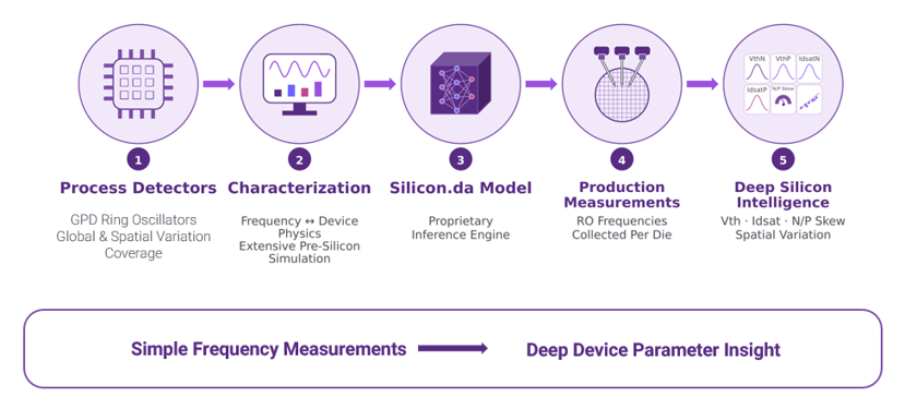
The emerging paradigm shifts towards 'design-aware' monitor analytics, moving beyond generic ring oscillators to purpose-built process detectors. These new monitors are not generic test structures but are specifically designed to probe particular device behaviors or process parameters that are critical for the target application. Instead of a single, aggregate frequency, these detectors can yield multiple, distinct measurements that correlate directly with specific physical phenomena.
Consider a scenario where a chip design is sensitive to both variations in transistor leakage current and variations in interconnect resistance. A conventional ring oscillator might show a change in frequency, but it would be ambiguous whether the primary driver was leakage or interconnects. A purpose-built detector, however, could include structures that independently measure these two parameters. For instance, one structure might be designed to be highly sensitive to leakage variations, while another is optimized to reflect changes in metal line resistance. By analyzing the outputs from both, designers and process engineers gain a much clearer picture of what is actually changing on the wafer.
This approach allows for a more nuanced understanding of process variability. It enables engineers to identify the specific root causes of deviation, rather than just observing the symptoms. This granular insight is crucial for optimizing manufacturing processes, improving yield, and achieving target device performance more consistently. The goal is to move from a 'one-size-fits-all' monitoring strategy to a 'precision-tuned' approach tailored to the specific sensitivities of the chip design and the manufacturing process itself.
Connecting Pre-Silicon Expectations to Production Reality
A key innovation in this new approach is the explicit connection between pre-silicon simulation and post-silicon measurements. Before a chip is even fabricated, sophisticated process design kits (PDKs) and simulation tools are used to model how variations in manufacturing parameters will affect device behavior. These models generate expectations for how different test structures should perform under various process conditions. Purpose-built process detectors are designed to generate measurements that can be directly compared against these pre-silicon simulations.
This comparison acts as a powerful feedback mechanism. If the measurements from the purpose-built detectors on the actual silicon deviate significantly from the pre-silicon predictions, it signals a discrepancy between the manufacturing model and reality. This discrepancy could stem from inaccuracies in the process models themselves, unexpected interactions during fabrication, or issues with the test structures or measurement equipment. Regardless of the cause, the ability to directly compare simulation with measured silicon behavior provides invaluable data for refining both the design models and the manufacturing process.
This closed-loop system is akin to a highly sophisticated weather forecasting model that not only predicts the weather but also continuously recalibrates its predictions based on real-time sensor data from across the globe. Without this continuous recalibration, forecasts quickly become inaccurate. Similarly, without linking silicon measurements back to pre-silicon expectations, process models and design guardbands remain static and potentially suboptimal. The integration of design-aware monitor analytics allows for dynamic adjustment and continuous improvement.
Implications for Design and Manufacturing
The adoption of purpose-built process detectors and design-aware analytics promises significant benefits across the semiconductor ecosystem. For chip designers, it means the potential to reduce guardbands, leading to higher performance, lower power consumption, and smaller die areas. By understanding the true sources of variation, designers can implement more targeted design-for-manufacturing (DFM) techniques and statistical design rules. This allows them to push the performance envelope closer to theoretical limits without sacrificing reliability.
For process engineers and yield enhancement teams, these detectors provide a much sharper diagnostic tool. They can pinpoint specific process steps or parameters that are causing deviations, enabling faster and more effective root cause analysis. This leads to improved process control, higher manufacturing yields, and reduced costs associated with wafer scrap and re-processing. The ability to identify issues earlier in the fabrication flow also contributes to this efficiency.
The industry is moving towards a future where silicon monitoring is an integral part of the design flow, not merely an afterthought for test. This evolution is driven by the increasing complexity of semiconductor manufacturing and the insatiable demand for higher performance and greater efficiency. As process nodes continue to shrink and device architectures become more intricate, the 'one-size-fits-all' approach of conventional ring oscillators will become increasingly inadequate. The future lies in intelligent, purpose-built monitoring that bridges the gap between the simulated world of pre-silicon design and the tangible reality of fabricated silicon.