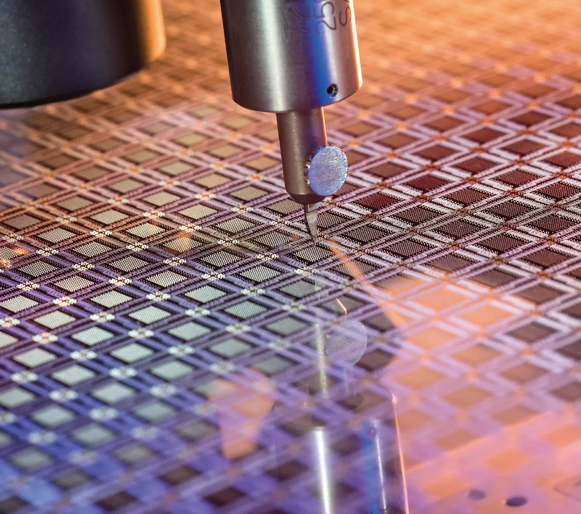
The Evolving Challenge of Semiconductor Interconnects
The relentless march toward higher integration in semiconductor manufacturing presents a growing challenge for ensuring the long-term reliability of interconnects. As chip densities increase, the physical space available for bonding pads shrinks, and the complexity of the interconnections grows. This miniaturization and intensification put unprecedented pressure on the physical connections, or bonds, that link the silicon die to its packaging. Traditional bond testing methodologies, often designed for less dense and less complex architectures, are increasingly proving insufficient to accurately assess the integrity and predict the lifespan of these critical connections.
Bond testing is no longer a mere quality check; it has emerged as a critical control point for maintaining long-term performance and maximizing yield. The consequences of bond failures can range from intermittent glitches and reduced device lifespan to catastrophic failures, all of which translate directly to increased costs and diminished market competitiveness. The industry is at an inflection point, requiring a fundamental re-evaluation of how bond reliability is measured and managed in the face of these escalating demands.
Why Traditional Methods Are Falling Short
The core issue lies in the scaling mismatch between advanced semiconductor designs and established testing protocols. As the number of connections per unit area increases, so does the potential for subtle defects that can propagate over time. These defects might include minute variations in bond strength, partial voids, or micro-cracks that are not immediately detectable by conventional tests. These tests often rely on static force or simple electrical continuity checks, which may not adequately stress the bonds to reveal latent weaknesses that will manifest under operational conditions.
Consider the analogy of building a skyscraper with microscopic support beams. A simple visual inspection might suggest everything is in place, but a subtle shift in load or a minor tremor could reveal weaknesses in the connections between these minuscule beams. Similarly, high-density semiconductor bonds require testing that simulates the dynamic stresses and environmental factors they will encounter throughout their operational life, not just a static snapshot of their initial state. The pressure is literally on, both physically on the bonds and figuratively on the manufacturers to ensure their products perform reliably.
The Need for Advanced Testing Techniques
To address these limitations, the industry is exploring and implementing more sophisticated bond testing techniques. These advanced methods aim to provide a more comprehensive understanding of bond integrity by incorporating dynamic stress, environmental simulation, and advanced inspection technologies. One key area of development is the use of dynamic mechanical testing, which applies controlled, varying forces to the bonds to mimic the stresses induced by thermal cycling and operational vibrations. This approach is far more effective at uncovering weaknesses that static pull tests might miss.
Furthermore, non-destructive evaluation (NDE) techniques are gaining prominence. Technologies such as advanced ultrasonic imaging and X-ray microscopy can peer inside the bond interface without damaging the component. These methods allow for the detection of internal voids, delamination, and material inconsistencies that are invisible to surface-level inspections. The goal is to move beyond simply verifying a connection exists to understanding the quality and robustness of that connection at a microscopic level.
Integrating Testing into the Manufacturing Workflow
The shift in bond testing is not just about adopting new tools; it's about fundamentally integrating these advanced assessments into the manufacturing workflow. Instead of being an end-of-line check, bond reliability evaluation needs to become a continuous process, providing feedback loops to optimize bonding processes in real-time. This proactive approach allows for early detection and correction of process deviations that could lead to yield loss or long-term reliability issues. The data generated from these advanced tests can inform adjustments to bonding parameters, such as temperature, pressure, and duration, ensuring that each bond is formed optimally for its specific context within the high-density chip.
What nobody has explicitly detailed yet is the investment required for such a comprehensive integration. While the benefits of improved yield and reliability are clear, the capital expenditure for advanced testing equipment, coupled with the need for specialized training for technicians and engineers, represents a significant hurdle. Companies must carefully weigh this investment against the escalating costs of field failures and product recalls in an increasingly competitive market.
The Future of Bond Reliability
The future of semiconductor manufacturing hinges on the ability to reliably connect ever-increasing numbers of components within shrinking footprints. This necessitates a paradigm shift in how bond reliability is understood and tested. The move towards dynamic, non-destructive, and integrated testing methods is not merely an upgrade; it's an essential evolution to keep pace with the demands of next-generation electronics. By embracing these advanced techniques, manufacturers can build greater confidence in the long-term performance of their high-density semiconductors, ensuring that precision is maintained even under the immense pressures of modern chip design.