Samsung Unveils zHBM: A Leap in AI Memory Integration
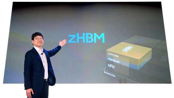
Samsung has introduced a prototype of its next-generation High Bandwidth Memory (HBM), dubbed zHBM, which represents a fundamental shift in how memory interacts with AI accelerators. Unlike traditional architectures where HBM stacks are placed adjacent to the main processing unit, zHBM integrates the memory dies directly on top of the AI chip. This novel approach aims to drastically reduce latency and increase bandwidth, critical factors for the insatiable demands of modern artificial intelligence workloads.
The current generation of AI accelerators, such as GPUs and custom ASICs, rely on external memory solutions. These solutions, while advanced, introduce physical distance between the processor and the memory. Data must travel across interposers and intricate packaging layers, creating bottlenecks and consuming significant power. Samsung's zHBM prototype directly addresses this by placing the memory dies in a monolithic stack atop the silicon reticle of the AI accelerator itself. This co-packaged approach minimizes the physical path data must traverse, leading to potentially orders-of-magnitude improvements in effective bandwidth and a substantial reduction in energy consumption per bit moved.
Think of it less like a supercomputer with a fast network connection between its CPU and RAM, and more like a brain where the short-term memory is literally built into the neurons. This tight integration is what zHBM promises for AI chips.
Technical Underpinnings and Potential Benefits
The key innovation behind zHBM lies in Samsung's advanced packaging technology. By stacking memory dies directly onto the AI accelerator reticle, the company eliminates the need for a separate silicon interposer, a common component in current advanced packaging solutions like chiplets and 2.5D integration. This direct stacking allows for a much denser connection between the memory and the processor. Samsung is leveraging its expertise in 3D V-NAND technology and advanced packaging techniques to achieve this integration. The prototype showcases the potential for significantly increased memory capacity and bandwidth within a smaller physical footprint.
For AI workloads, especially large language models (LLMs) and complex deep learning training and inference tasks, memory bandwidth and latency are often the primary performance inhibitors. Training models with billions or trillions of parameters requires moving vast datasets in and out of memory at extremely high speeds. Inferencing, while generally less demanding than training, still benefits immensely from low-latency memory access to provide real-time responses. zHBM's architecture is designed to alleviate these bottlenecks. By bringing the memory physically closer to the compute cores, it slashes the distances data must travel, thereby reducing signal propagation delays and power overhead associated with data movement.
Samsung has not yet disclosed the exact specifications of the zHBM prototype, such as the number of memory dies stacked or the specific bandwidth figures achieved. However, the implications of such a design are profound. If successful, it could lead to AI accelerators that are not only faster but also more power-efficient, a critical consideration for data centers facing increasing energy demands and sustainability pressures. The reduced power consumption per operation is a direct consequence of minimizing the physical distance data travels. Moving data over shorter distances requires less energy, and when dealing with the exabytes of data processed by AI systems, these savings can be substantial.
Market Context and Future Implications
The AI hardware market is fiercely competitive, with companies like NVIDIA, AMD, Intel, and numerous AI chip startups constantly pushing the boundaries of performance. Memory technology is a critical battleground in this race. The development of HBM has been instrumental in enabling the massive memory capacities and bandwidths required for advanced AI. HBM3 and HBM3E are current industry standards, offering significant improvements over their predecessors. Samsung's zHBM, however, represents a potential paradigm shift beyond incremental improvements, moving towards a more deeply integrated compute and memory architecture.
This move by Samsung aligns with broader industry trends towards advanced packaging and heterogeneous integration. The concept of