
AI Accelerates Custom Silicon Design
OpenAI has revealed a significant internal development: the successful design of its custom silicon, codenamed "Jalapeño," was substantially aided by its own large language models (LLMs). This initiative represents a pivotal moment, showcasing the burgeoning capability of AI to not only generate software and text but also to contribute meaningfully to the complex, hardware-centric field of chip design. The project aimed to create specialized hardware optimized for AI workloads, a move that could reduce reliance on third-party chip manufacturers and potentially offer performance advantages.
The design process for modern integrated circuits is notoriously intricate, involving millions of design rules, complex optimization algorithms, and vast search spaces. Traditionally, this has been the domain of highly specialized human engineers. OpenAI's approach, however, integrated LLMs directly into this workflow. The models were trained on extensive datasets encompassing chip design principles, existing chip architectures, and performance metrics. This allowed them to assist in tasks ranging from high-level architectural exploration to detailed layout optimization.
One of the key challenges in chip design is exploring the immense design space to find optimal configurations that balance performance, power consumption, and area (PPA). LLMs, with their ability to process and generate complex, structured information, proved adept at navigating this space. They could suggest novel architectural variations, identify potential bottlenecks early in the design cycle, and even propose solutions for complex routing and placement problems that might elude human designers working with conventional tools.
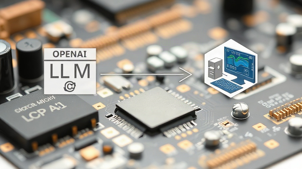
LLM-Assisted Design Workflow
The Jalapeño project employed a multi-stage process where LLMs were integrated at various points. Initially, the models were used for architectural exploration, generating potential block diagrams and evaluating trade-offs between different design choices. This phase is critical, as fundamental architectural decisions made early on have ripple effects throughout the entire design process. By leveraging LLMs, OpenAI could explore a wider array of architectural possibilities in a shorter timeframe than would be feasible with human-only efforts.
Following architectural definition, the LLMs assisted in the synthesis and verification stages. For synthesis, they helped in translating high-level design descriptions into lower-level hardware descriptions (like Verilog or VHDL), ensuring adherence to complex design rules. Verification, a notoriously time-consuming part of chip design, also benefited. The LLMs could generate test cases, analyze simulation results, and even identify subtle bugs or potential issues that might be missed by standard verification methodologies. This iterative process of design, synthesis, and verification, powered by AI, allowed for rapid prototyping and refinement.
This method is akin to having an incredibly knowledgeable, albeit specialized, co-pilot for every engineer. Instead of manually sifting through documentation or running countless simulations to test a hypothesis, engineers could query the LLM, receive suggestions, and then use traditional tools to validate and implement those suggestions. The LLMs acted as intelligent assistants, augmenting human expertise rather than replacing it entirely. The surprising detail here is not merely that LLMs *can* assist, but that OpenAI successfully integrated them into the core, performance-critical stages of actual custom silicon design, moving beyond theoretical exploration.
Implications for AI Hardware and Beyond
The successful design of Jalapeño using LLMs has profound implications for the future of AI hardware development. It suggests a potential paradigm shift where AI models become integral tools not just for software development but for the creation of the very hardware that runs AI. This could accelerate innovation cycles, allowing companies to develop more specialized and efficient chips tailored to specific AI tasks, whether for training large models or for efficient inference in deployed systems.
For companies like OpenAI, developing custom silicon offers several strategic advantages. It provides greater control over the hardware roadmap, enabling optimization for their specific software stack and workloads. This can lead to significant performance gains and cost efficiencies compared to relying on general-purpose hardware. Furthermore, it represents a step towards greater vertical integration, a trend seen across the AI industry where leading players are increasingly controlling both the software and hardware layers of their operations.
The broader impact extends to the semiconductor industry. While traditional chip design houses possess decades of expertise and sophisticated toolchains, the success of this AI-driven approach could spur further research and investment in similar methodologies. It raises questions about the future role of human chip designers and the evolution of electronic design automation (EDA) tools. Will AI-generated chip designs become the norm? What new types of architectures will emerge when design constraints are explored by intelligences that do not share human cognitive biases?
This development underscores a broader trend: the increasing sophistication of AI capabilities moving beyond abstract tasks into the realm of physical product design and manufacturing. As LLMs become more adept at understanding and generating complex, structured information, their application in fields like material science, drug discovery, and engineering design is likely to expand dramatically.