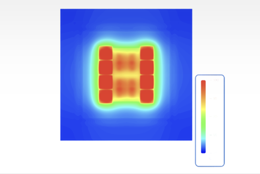
The Challenge of Thermal Management in Advanced AI Packages
Modern AI accelerators, particularly those employing 2.5D and 3D packaging, present unprecedented thermal challenges. The drive for higher performance and greater integration density means more transistors are packed into smaller footprints, leading to significantly increased power density. This concentrated heat generation can create hotspots, degrade performance, and reduce the reliability and lifespan of the entire package. Traditional thermal simulation methods, while accurate, are computationally intensive and time-consuming. They often operate at speeds far slower than the design iterations required during the early stages of chip development, creating a bottleneck. This disconnect forces designers to make critical decisions about die and package architecture with incomplete thermal data, or to rely on simplified, less accurate models. The result is often over-engineering to meet thermal budgets, leading to larger, more expensive, and less power-efficient designs, or worse, designs that fail to meet performance targets due to thermal throttling.
Introducing Floorplanning-Speed Full-Fidelity Thermal Simulation
Semiconductor Engineering's latest research addresses this critical gap by developing a full-fidelity thermal simulation technique that operates at speeds comparable to the floorplanning stage of chip design. This breakthrough allows engineers to perform detailed thermal analysis concurrently with architectural decisions, rather than as a post-design verification step. The new method achieves this by leveraging advanced numerical techniques and computational shortcuts that maintain a high degree of accuracy while dramatically reducing simulation time. Instead of simulating every single component at an atomic level, it intelligently models thermal behavior based on aggregated power densities and material properties, effectively treating large blocks of the design as single thermal entities where appropriate, without sacrificing the ability to identify localized hotspots.

Key Innovations and Methodologies
The core of this new simulation approach lies in its hybrid modeling strategy. It combines a fast, coarse-grained simulation for overall thermal distribution with a localized, fine-grained simulation that can be invoked on demand for critical areas identified by the coarse model. This is analogous to how a weather forecast provides a general outlook for a large region, but can zoom into specific cities for more detailed predictions during a storm.
Furthermore, the technique incorporates machine learning models trained on vast datasets of previous simulations. These models learn the complex relationships between power maps, material stacks, and resulting temperature profiles. When presented with a new design, the ML components can rapidly predict thermal behavior, guiding the more computationally expensive physics-based simulations to focus only on the most sensitive regions. This drastically reduces the computational overhead, bringing the simulation time down from hours or days to minutes, aligning it with the pace of floorplanning and early architectural exploration.
Co-Optimization of Die and Package Design
One of the most significant benefits of this floorplanning-speed simulation is its ability to enable true co-optimization of die and package design. In traditional workflows, the die is designed first, and then the package is engineered to manage its thermal output. This often leads to suboptimal solutions. With the new simulation technique, designers can explore various die configurations and interposer designs, alongside different package materials and cooling solutions, simultaneously. They can dynamically adjust power delivery networks, thermal vias, and heat spreaders while observing the immediate thermal impact. This iterative process allows for the identification of synergistic improvements, where changes in the die layout might reduce the burden on the package, or vice-versa, leading to a more holistically optimized and thermally efficient final product. It moves beyond simply meeting a thermal budget to actively seeking the most performant and efficient design within that budget.
Impact on AI Accelerator Development
The implications for AI accelerator development are profound. Engineers can now explore a much wider design space within their development timelines. This means:
- Mitigating Hotspots Early: Potential hotspot locations can be identified and addressed in the initial floorplan, preventing costly redesigns later in the cycle.
- Optimizing Thermal Budgets: Designers can push the boundaries of power density more aggressively, knowing they have a tool that can accurately predict and manage the resulting heat. This allows for smaller, more powerful chips.
- Reducing Design Iterations: The accelerated simulation cycle significantly shortens the overall design time, enabling faster time-to-market for new AI hardware.
- Improving Reliability and Performance: By ensuring designs operate within safe thermal limits, the longevity and consistent performance of AI accelerators are enhanced.
This advancement is particularly critical for heterogeneous integration strategies, such as chiplets and advanced 2.5D/3D stacking, where thermal interactions between different components are complex and highly interdependent. The ability to simulate these interactions at speed is no longer a luxury but a necessity for competitive AI hardware development.