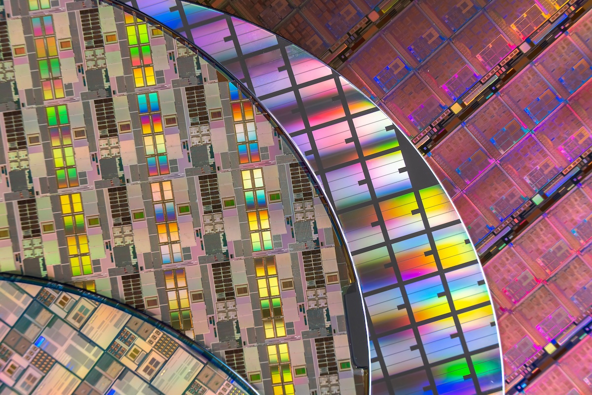
Micron Expands Research Capabilities with New Lab

Micron Technology has inaugurated a new state-of-the-art laboratory, signaling a commitment to accelerated innovation in memory and storage solutions. While specific details on the lab's focus remain under wraps, such investments are critical for pushing the boundaries of data density, performance, and energy efficiency in DRAM and NAND flash technologies. This move positions Micron to better tackle future memory challenges, particularly those driven by the insatiable demands of artificial intelligence and high-performance computing. The lab's existence suggests a proactive approach to addressing the evolving needs of the semiconductor market, where memory is increasingly becoming a performance bottleneck.

AI Chip Costs Surge as Demand Outstrips Supply

The cost of specialized chips for artificial intelligence applications has seen a significant jump, reflecting a widening gap between burgeoning demand and constrained supply. This price escalation is a direct consequence of the exponential growth in AI model training and inference workloads, which require increasingly powerful and specialized silicon. Foundries are operating at maximum capacity, and the lead times for advanced process nodes are stretching. Companies developing AI hardware are facing intense pressure to secure manufacturing slots, leading to higher component costs that are inevitably passed on to end-users and cloud providers. This trend highlights the critical need for expanded manufacturing capacity and further investment in diverse AI chip architectures to alleviate the bottleneck.

Advancements in Multi-Die Monitoring and Interconnects

Innovations in monitoring technologies for multi-die systems are becoming paramount as chip architectures increasingly adopt heterogeneous integration and chiplet designs. Ensuring the reliability and performance of systems comprising multiple interconnected dies requires sophisticated, real-time monitoring solutions. These systems must track thermal conditions, power delivery, and signal integrity across disparate components. Simultaneously, the interconnect between these dies presents a significant bottleneck. The interconnect RC (Resistance-Capacitance) delay is a key limiter for performance in advanced packaging. Researchers are actively exploring novel materials and routing strategies to mitigate this issue, aiming to enable faster, more efficient communication between chiplets. This work is foundational for realizing the full potential of advanced packaging technologies.

Cryogenic Links for Quantum Computing Emerge

The pursuit of stable and scalable quantum computing has seen a notable development in the exploration of cryogenic links for quantum chips. Maintaining qubits at extremely low temperatures is essential for their delicate quantum states. Efficiently connecting and controlling these qubits, especially in larger-scale quantum processors, requires specialized interconnects that can operate reliably in a cryogenic environment without introducing noise or heat. Advances in this area are crucial for building more robust and powerful quantum systems. The challenge lies in creating high-density, low-loss connections that can be scaled alongside the number of qubits.

Intel Secures 18A Process Node Milestone

Intel has announced a significant achievement, securing an '18A win,' indicating progress with its 18 Angstrom (1.8nm) process technology. This node represents a critical step forward in transistor technology, aiming for higher density and improved performance. Success with such advanced process nodes is vital for maintaining competitiveness in the CPU and GPU markets, as well as enabling next-generation AI accelerators. The race to shrink transistor sizes and improve their efficiency is a perpetual one in the semiconductor industry, and Intel's advancement with 18A positions it to compete more effectively with other leading foundries.

CPO Roadmap and New Leadership

Co-Packaged Optics (CPO) continues to be a focus, with roadmaps being laid out for its integration into future networking and computing systems. CPO promises to bring optical connectivity closer to the silicon, reducing power consumption and increasing bandwidth for data-intensive applications. In parallel, the industry has seen the appointment of two new CEOs, reflecting ongoing leadership transitions and strategic realignments within key semiconductor companies. Such leadership changes often signal shifts in corporate strategy, R&D focus, and market approach.

Humanoid Robot Readiness Gap

Beyond the silicon itself, the broader ecosystem for advanced technologies is also evolving. A notable observation is the existing 'humanoid readiness gap.' While AI and robotics hardware are advancing rapidly, the infrastructure, software, and deployment strategies necessary for widespread adoption of humanoid robots are still in their nascent stages. This gap suggests that the physical integration and application of advanced chips into real-world robotic systems will require significant parallel development in areas like control systems, power management, and human-robot interaction. What nobody has addressed yet is the timeline and investment required to bridge this gap effectively across various industries.

Hot Interconnects Conference Highlights

The recent Hot Interconnects conference showcased cutting-edge research in interconnect technologies. Discussions likely covered novel architectures, high-speed signaling techniques, and power-efficient communication protocols essential for modern computing systems, from data centers to edge devices. This forum serves as a critical venue for researchers and engineers to share advancements that will shape the future of how chips communicate with each other and the outside world.