The Challenge of Advanced Semiconductor Packaging
As semiconductor devices shrink and integration density increases, the challenges of managing thermal expansion and electromigration become paramount. These phenomena, driven by increasing power densities and complex material stacks within advanced packages, can lead to device failure and reduced lifespan. Traditional approaches to managing these issues often involve compromises in performance or significant increases in manufacturing cost and complexity. The need for novel solutions in interposer design is therefore critical to unlocking the full potential of next-generation integrated circuits.
Thermal expansion, the tendency of materials to change volume in response to temperature changes, becomes a significant problem when different materials with varying coefficients of thermal expansion (CTE) are bonded together. In advanced semiconductor packaging, such as 2.5D and 3D integration, multiple layers of silicon, dielectrics, and metals are stacked. When these devices operate, localized heating occurs, leading to differential expansion. This can induce stress at interfaces, causing delamination, cracking, or even catastrophic failure. For instance, a silicon interposer bonded to a substrate with a significantly different CTE will experience considerable mechanical stress during operation. Managing this stress is not just about preventing immediate failure; it's about ensuring long-term reliability and predictable performance under varying operating conditions.
Electromigration, on the other hand, is a physical phenomenon where the gradual movement of ions in a conductor occurs due to the momentum transfer between electrons and the metal atoms. In high-current density environments, such as those found in advanced interconnects and power delivery networks within integrated circuits, electromigration can lead to the formation of voids or hillocks. Voids can break the electrical connection, leading to open circuits, while hillocks can cause short circuits. The smaller the feature sizes and the higher the current densities, the more susceptible the device becomes to electromigration-induced failures. This is particularly relevant in the fine-pitch interconnects enabled by advanced lithography and packaging technologies.
Interposer Design Strategies for Mitigation
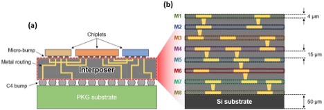
Addressing these intertwined challenges requires a multi-faceted approach, with interposer design playing a central role. The interposer acts as a bridge between the chip and the package substrate, and its material properties, geometry, and thermal management features are key determinants of overall system reliability.
One primary strategy involves careful selection of interposer materials and their integration with adjacent layers. While silicon is a common choice for its excellent electrical properties and established manufacturing processes, its CTE needs to be carefully managed. Alternative interposer materials, or composite structures, can be employed to better match the CTE of the package substrate, thereby reducing interfacial stress. This might involve using organic interposers, glass, or even advanced ceramic materials, each with its own set of advantages and disadvantages regarding thermal conductivity, electrical performance, and cost.
Geometric design of the interposer also offers avenues for stress relief. Features such as strategically placed trenches, varying thicknesses, or the incorporation of compliant layers can help absorb or redistribute the mechanical stresses induced by thermal expansion. The layout of interconnects on the interposer is equally critical for electromigration. Designers must optimize trace widths, lengths, and routing to minimize current density hotspots. Techniques like using wider traces for high-current paths, employing redundant interconnects, and implementing specific via structures can significantly enhance electromigration resistance.
Thermal management is intrinsically linked to both thermal expansion and electromigration. Efficient heat dissipation from the interposer and the stacked chips is crucial. This can be achieved through various means, including the integration of thermal vias directly within the interposer, the use of high thermal conductivity materials for the interposer itself, and optimizing the thermal interface materials (TIMs) between the chip, interposer, and package. Advanced simulation techniques, including those leveraging deep learning models, are becoming indispensable for accurately predicting thermal profiles and stress distributions under various operating conditions. These models can help identify potential failure points early in the design cycle, allowing for proactive design modifications.
The excerpt mentions new deep learning models for modeling warpage. This points to a significant trend in the industry: the application of AI and machine learning to solve complex engineering problems that were previously intractable with traditional physics-based simulations alone. For warpage, which is a macroscopic manifestation of differential thermal expansion, deep learning can potentially predict deformation more rapidly and accurately by learning from vast datasets of simulation results or experimental measurements. This is akin to having an experienced engineer who can intuitively estimate the outcome of a complex design, but powered by computational might.
Referenced Sources
- verified