Intel's Strategic Bet on In-House Photomask Production
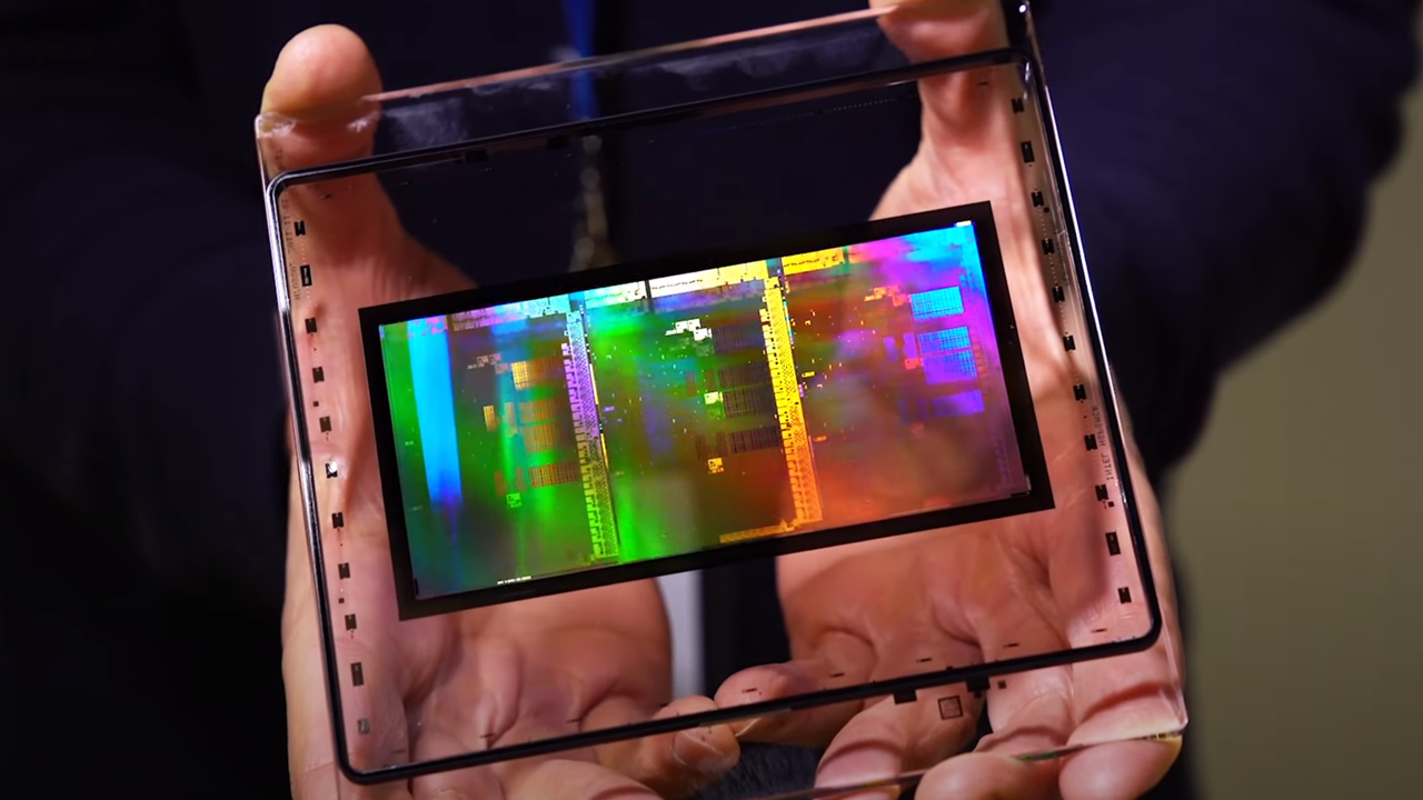
Intel is undertaking a significant expansion of its photomask manufacturing capabilities at its Bowers Campus in Santa Clara, California. This move underscores the company's commitment to bolstering its internal production of these critical components, essential for the fabrication of increasingly sophisticated semiconductor chips. As process nodes shrink and lithography techniques become more complex, particularly with the advent of Extreme Ultraviolet (EUV) and High-NA EUV (High Numerical Aperture EUV) lithography, the precision and quality of photomasks are paramount. By bringing more of this specialized manufacturing in-house, Intel aims to gain greater control over its supply chain, accelerate innovation, and ensure access to the most advanced mask technology required for next-generation processors.
Photomasks are essentially the stencils used in photolithography to transfer circuit patterns onto silicon wafers. They are incredibly intricate, high-precision tools, often costing millions of dollars each, especially those designed for EUV lithography. The transition to EUV, which uses shorter wavelengths of light (13.5 nm compared to traditional deep ultraviolet wavelengths), allows for the printing of much finer features on chips, enabling higher transistor density and improved performance. High-NA EUV represents the next evolutionary leap, promising even greater resolution and the ability to pattern smaller features, crucial for advanced nodes like Intel 18A and beyond.
The decision to expand photomask production at the Bowers Campus is not merely about increasing volume; it's about mastering the complex technologies that underpin these advanced nodes. Producing EUV masks, which are reflective rather than transmissive and require specialized materials and defect inspection techniques, is a considerable engineering challenge. High-NA EUV masks introduce further complexities due to their larger size and the need for even tighter tolerances. Intel's investment here suggests a long-term strategy to reduce reliance on external mask shops, which may struggle to keep pace with the demands of leading-edge chip manufacturing, and to foster a deeper internal understanding and development of mask technologies.
The Critical Role of Photomasks in Advanced Lithography
Photomasks are the linchpins of semiconductor manufacturing. For decades, their production has been a specialized field, often outsourced to dedicated companies. However, as chip designs become more intricate and the lithographic tools more advanced, the photomask itself becomes a bottleneck and a critical source of competitive advantage. The transition from DUV to EUV lithography was a monumental undertaking for the entire semiconductor industry, and photomask production was at the heart of this challenge.
EUV masks present unique difficulties. Unlike traditional masks that transmit light through a quartz plate, EUV masks use a reflective multilayer coating. This means any defect can reflect the EUV light, potentially ruining the pattern transfer. Furthermore, the shorter wavelength of EUV light means that even microscopic defects on the mask can translate into significant flaws on the silicon wafer. Detecting and repairing these defects on EUV masks requires highly specialized equipment and expertise.
The next frontier, High-NA EUV, takes these challenges to a new level. High-NA EUV scanners, like those being developed by ASML, use a larger optical lens system with a higher numerical aperture. This allows for finer feature patterning but also requires larger photomasks to capture the expanded field of view. These larger masks, coupled with the increased precision required for High-NA EUV patterning, demand even more stringent control over mask flatness, material uniformity, and defect management. Intel's explicit focus on both EUV and High-NA EUV in its expansion indicates a forward-looking strategy, positioning the company to leverage these technologies as soon as they become fully viable for high-volume manufacturing.
Why In-House Production Matters for Intel
Intel's strategic decision to expand its in-house photomask production is multifaceted. Firstly, it provides a significant degree of supply chain security. Relying on external vendors for such critical, high-tech components can introduce risks related to availability, lead times, and intellectual property protection. By controlling its own mask supply, Intel can better manage production schedules and mitigate potential disruptions.
Secondly, it fosters a closer feedback loop between chip design, process development, and mask manufacturing. When these functions are co-located or tightly integrated, engineers can iterate more rapidly on mask designs, address manufacturing challenges proactively, and optimize the entire process from chip layout to wafer fabrication. This synergy is particularly important for bleeding-edge process nodes where subtle mask imperfections can have outsized impacts on yield and performance.
Thirdly, it positions Intel to be a leader in developing and implementing next-generation mask technologies. The nuances of High-NA EUV mask production are still being explored and refined. By investing heavily in its own capabilities, Intel can contribute to this evolution, potentially setting new industry standards and gaining a competitive edge. This is akin to a chef cultivating their own rare ingredients to ensure the highest quality and unique flavor in their dishes, rather than relying solely on what the market provides.
The expansion at the Bowers Campus is not a minor upgrade; it represents a substantial commitment to the future of semiconductor manufacturing. It signals Intel's intent to not only adopt the most advanced lithography techniques but also to master the foundational elements that enable them. This strategic move is a clear indicator of Intel's long-term vision to regain its manufacturing leadership and drive innovation across the semiconductor industry.
Broader Industry Implications
Intel's investment in in-house photomask production for EUV and High-NA EUV has significant implications for the broader semiconductor ecosystem. For years, the industry has seen a concentration of photomask expertise within a few specialized companies. Intel's move could signal a trend towards greater vertical integration among leading foundries and Integrated Device Manufacturers (IDMs) seeking to secure their supply of these vital components.
This could put pressure on existing photomask suppliers to innovate faster, improve their capacity, and potentially differentiate themselves through specialized services or technologies. It also highlights the immense cost and complexity associated with advanced semiconductor manufacturing, where every step of the process, from chip design to the very stencils used to pattern wafers, requires massive investment and cutting-edge expertise.
For the development of High-NA EUV, Intel's enhanced in-house capabilities could accelerate the path to high-volume manufacturing. Close collaboration between Intel's engineers and ASML (the sole supplier of EUV and High-NA EUV lithography tools) becomes more feasible when Intel has deep expertise and production capacity for the associated masks. This integrated approach is essential for ironing out the kinks in a nascent technology that promises to define the future of chipmaking.
Ultimately, Intel's expansion in California is more than just a facility upgrade; it's a strategic play to secure its manufacturing future, drive technological advancement, and reinforce its position as a leader in the relentless pursuit of smaller, faster, and more powerful semiconductors.