Intel's 18A Node: A Critical Juncture
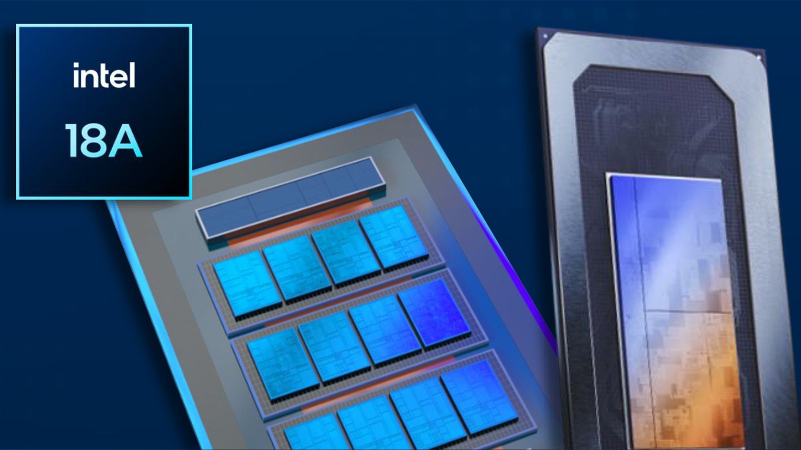
Intel's pursuit of manufacturing process leadership has reached a critical juncture with its 18A node. This advanced process technology is central to the company's 'IDM 2.0' strategy, aiming to reclaim its foundry crown and compete more aggressively with TSMC and Samsung. The 18A node, particularly significant for its use of RibbonFET and PowerVia technologies, is intended to enable Intel to deliver chips with performance advantages that don't require additional packaging layers. However, the path to high-volume manufacturing for such advanced nodes is fraught with technical hurdles, and early reports indicated that Intel was grappling with significant yield issues, particularly concerning wafer-to-wafer (W2W) bonding. A recent report from Tom's Hardware, citing industry sources, now suggests that Intel has successfully addressed these critical W2W yield problems, a development that, if accurate, could significantly alter the competitive landscape in advanced semiconductor manufacturing.
Understanding the 18A Node and Its Challenges
The 18A process is Intel's most advanced node, slated for use in its own future processors and for its foundry customers. It represents a leap forward, incorporating two key innovations: RibbonFET, Intel's new gate-all-around transistor architecture, and PowerVia, a backside power delivery system. RibbonFET aims to provide better electrostatic control over the channel, leading to improved performance and power efficiency compared to traditional FinFETs. PowerVia, on the other hand, decouples power delivery from the front side of the chip, allowing for shorter signal paths and potentially denser transistor layouts. This combination is designed to offer a significant performance-per-watt advantage. However, the integration of these cutting-edge technologies, especially the wafer-to-wafer bonding required for PowerVia, presents immense manufacturing complexity. W2W bonding involves precisely aligning and joining two wafers, which requires sub-micron accuracy and pristine surface conditions. Any imperfections or misalignment can lead to catastrophic failures, dramatically impacting yield. Early in its development, the 18A node reportedly suffered from low yields, with W2W bonding identified as a primary culprit. Overcoming these challenges is not merely an incremental improvement; it's a fundamental requirement for the node's viability and Intel's broader strategic ambitions.
Reported Breakthrough in Wafer-to-Wafer Yield
The core of the recent report centers on Intel's alleged success in resolving the intractable wafer-to-wafer yield issues that have plagued the 18A process. While the specifics of the fix are not detailed in the public report, it implies that Intel's engineering teams have found ways to improve the precision, cleanliness, and reliability of the W2W bonding process. This could involve advancements in metrology, defect reduction, equipment calibration, or process control. For a technology as complex as 18A, a breakthrough in W2W yield is akin to unlocking a critical bottleneck. It suggests that Intel is moving closer to achieving the high-volume manufacturing (HVM) targets necessary for its commercial deployment. The report also claims that production capacity for the 18A node has ramped up significantly, reaching up to 15,000 wafers per month at both of Intel's advanced manufacturing sites. This figure, if accurate, indicates a substantial increase from previous production levels and signals a growing confidence within Intel regarding the stability and scalability of the 18A process. Such a ramp-up is essential to meet the demand for next-generation chips, both for Intel's internal product roadmap and for its growing external foundry business.
Implications for Intel and the Semiconductor Industry
The implications of Intel successfully stabilizing its 18A node are far-reaching. For Intel, it represents a potential redemption and a crucial step in its turnaround plan. Reclaiming manufacturing superiority is not just about bragging rights; it's about enabling the performance and cost advantages needed to win back market share from competitors like AMD, particularly in the PC and server segments, and to attract lucrative foundry contracts. The 18A node is seen as Intel's ticket to competing at the leading edge against TSMC's N3 and N2 nodes and Samsung's upcoming processes. If Intel can indeed deliver competitive yields and performance at 18A, it could disrupt the established order of semiconductor manufacturing. This would provide Intel's foundry customers with a viable alternative to the duopoly of TSMC and Samsung, potentially leading to a more diversified and competitive foundry market. The success of 18A also validates Intel's aggressive R&D investment and its IDM 2.0 strategy, which combines internal manufacturing with external foundry services. It signals that Intel's internal process development is on track, a critical factor for investor confidence and future strategic planning. The surprise here is not just the claimed fix, but the potential speed at which Intel might be overcoming these deeply technical hurdles, a testament to the intense focus and resources dedicated to this program.
Lingering Questions and Future Outlook
While the news of fixed W2W yield issues for 18A is significant, it's important to acknowledge that this report is based on claims from unnamed industry sources. Intel itself has not officially confirmed these specific yield improvements or production volumes. Furthermore, even if the W2W bonding issues are resolved, the 18A node is a complex system, and other challenges related to materials, integration, or long-term reliability could still emerge. The true test will be the actual performance, power efficiency, and cost-effectiveness of chips manufactured on the 18A node when they reach the market. Intel has stated that its first products using the 18A process, such as the 'Arrow Lake' CPUs and 'Loon Creek' FPGAs, are expected to launch in the latter half of 2024 or early 2025. The performance and market reception of these products will be the ultimate arbiter of 18A's success. The critical question that remains unanswered is what happens to the competitive dynamics if Intel can genuinely achieve manufacturing parity or superiority with 18A. Will it be enough to significantly shift market share from established players, or will the high cost and complexity of bleeding-edge foundries continue to favor incumbents with decades of HVM experience? The industry will be watching closely as Intel moves from reported fixes to actual product shipments.