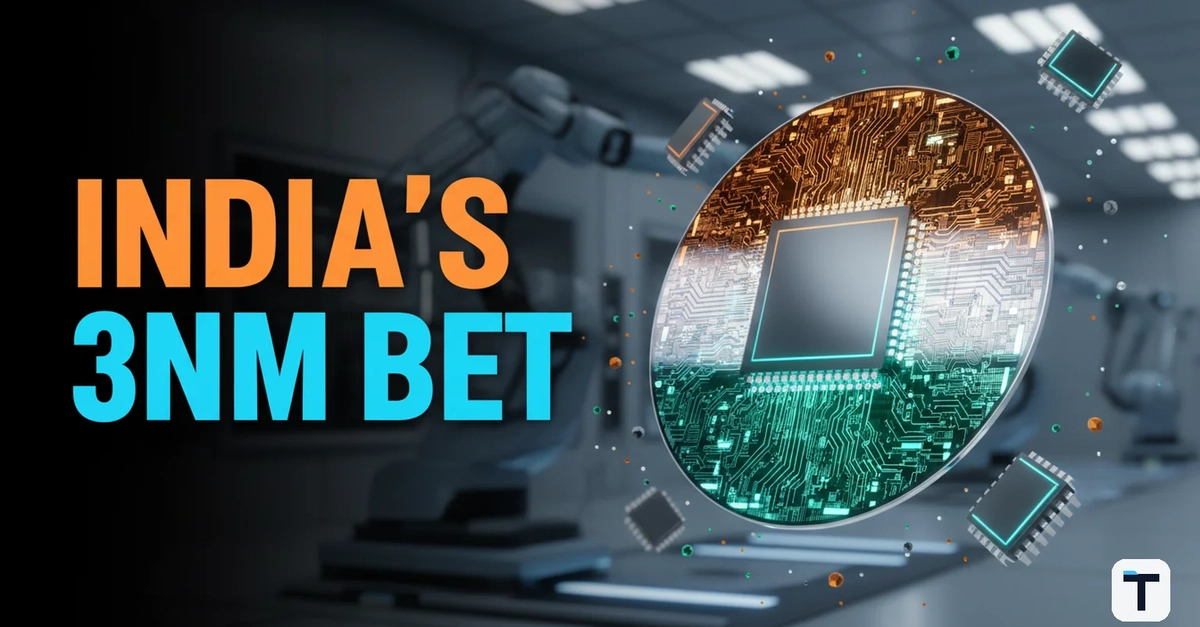
India's Ambitious Chip Roadmap: The Semicon 2.0 Vision
India's IT Minister Ashwini Vaishnaw has articulated a bold vision: the development of 7nm to 3nm chip technology within the next eight years. This ambitious goal is underpinned by Semicon 2.0, a recently approved program with a substantial investment of ₹1,27,500 crore. However, it's crucial to understand that this announcement outlines a technology roadmap, not an immediate production capability. India's sole existing semiconductor fabrication unit, SCL Mohali, currently operates at approximately 180nm process nodes. The country's first major commercial fab, a joint venture between Tata and PSMC in Dholera, is under construction and will focus on mature nodes, not leading-edge ones. The credibility of India's plan rests heavily on its strengths in chip design, talent development, and advanced packaging. Achieving leading-edge manufacturing, however, presents a genuinely formidable challenge.
The distinction between technology development and manufacturing is paramount. While India possesses a burgeoning ecosystem for chip design and a growing pool of skilled engineers, the capital-intensive and technologically complex nature of setting up and operating advanced semiconductor fabrication plants (fabs) for nodes like 3nm is a different ballgame. Companies like TSMC, Intel, and Samsung have spent decades and billions of dollars perfecting these processes. India's strategy appears to be a phased approach, leveraging its existing design strengths while gradually building manufacturing capacity, starting with more established nodes.
Understanding the Technology Targets
The target of 7nm to 3nm chip technology signifies a push into the most advanced semiconductor nodes currently in production or under development globally. These nodes are critical for high-performance computing, artificial intelligence, advanced mobile devices, and next-generation networking equipment. Achieving such miniaturization requires sophisticated lithography techniques, advanced materials, and incredibly precise manufacturing processes. For context, 3nm technology is already being deployed by leading foundries, offering significant improvements in performance and power efficiency compared to older nodes.
India's current capabilities, as represented by SCL Mohali, are far removed from these cutting-edge nodes. The focus on mature nodes for the new Tata-PSMC fab is a pragmatic step. Mature nodes, typically 28nm and above, are still vital for a vast array of products, including automotive electronics, power management ICs, and certain consumer electronics. By building capacity for these, India aims to reduce reliance on imports for essential components and foster a domestic semiconductor supply chain. The Semicon 2.0 program, therefore, appears to be a dual-pronged strategy: nurturing the design and talent pipeline for future advanced nodes while simultaneously building foundational manufacturing capabilities for current market demands.
The Role of Semicon 2.0 and Investment
The ₹1,27,500 crore (approximately $15 billion USD) allocated to Semicon 2.0 represents a significant government commitment to revitalizing India's semiconductor industry. This investment is expected to flow into various aspects of the semiconductor value chain, including:
- Research and Development: Funding for advanced research into new materials, processes, and architectures necessary for future nodes.
- Talent Development: Initiatives to train and upskill engineers and technicians in semiconductor design, fabrication, and testing.
- Design Ecosystem Support: Providing resources, tools, and potentially intellectual property access to facilitate chip design.
- Manufacturing Infrastructure: Incentives and support for setting up new fabrication plants, including those for advanced packaging.
- Assembly, Testing, and Packaging (ATP): Strengthening capabilities in the crucial post-fabrication stages, which are often less capital-intensive than wafer fabrication.
The success of Semicon 2.0 hinges on effective allocation and utilization of these funds. It requires a coordinated effort between government, industry, and academia to bridge the gap between design aspirations and manufacturing realities. The program's timeline of eight years for achieving 7nm-3nm technology is aggressive, especially considering the global race for semiconductor dominance.
Challenges and Opportunities Ahead
The path to developing 3nm chip technology is fraught with challenges. These include the immense cost of setting up and maintaining state-of-the-art fabs, the need for a highly specialized and skilled workforce, securing access to critical raw materials and equipment, and navigating complex global supply chains. Furthermore, the rapid pace of technological advancement means that by the time India establishes 3nm manufacturing, the global industry may already be moving towards 2nm or even sub-2nm nodes.
However, the opportunities are equally significant. India's large domestic market, growing digital economy, and increasing demand for electronics create a strong pull for local semiconductor production. A robust domestic semiconductor industry can enhance national security, reduce import dependence, create high-value jobs, and foster innovation across various sectors. The focus on design and packaging also presents a more accessible entry point, allowing India to carve out a niche in specific segments of the semiconductor value chain.
The government's emphasis on design and talent is a strategic advantage. India has a strong foundation in software and engineering talent, which can be leveraged for chip design. Advanced packaging technologies, which involve integrating multiple chips into a single package, are becoming increasingly important for performance gains and offer a more achievable manufacturing goal in the medium term. By excelling in these areas, India can become a significant player in the global semiconductor landscape, even if it takes longer to achieve leading-edge wafer fabrication.
What This Means for India's Semiconductor Future
India's 3nm chip roadmap, driven by Semicon 2.0, signals a long-term commitment to becoming a major player in the global semiconductor industry. While immediate production of 3nm chips is not on the horizon, the plan correctly identifies design, talent, and packaging as critical areas for initial focus. The substantial investment and clear technological targets set an ambitious benchmark. The journey from 180nm to 3nm is a marathon, not a sprint, and Semicon 2.0 represents the starting gun for India's pursuit of advanced semiconductor capabilities over the next decade.