The AI Imperative for Advanced Transistors
The insatiable hunger of artificial intelligence for processing power and energy efficiency is driving a fundamental shift in semiconductor design. Traditional transistor scaling, the engine of Moore's Law for decades, is hitting physical limits. To meet the demands of AI workloads, which involve massive parallel computations and constant data movement, the industry is rapidly advancing to new transistor architectures. Gate-All-Around (GAA) and Complementary Field-Effect Transistors (CFET) represent the leading edge of this evolution, promising significant improvements in performance, power consumption, and density. These aren't mere incremental upgrades; they are architectural shifts designed to unlock the next era of computing performance.
The challenge is that AI's computational needs are not just about raw speed. They also require immense energy efficiency. Training large language models and running inference on complex neural networks consumes vast amounts of power, contributing to significant operational costs and environmental concerns. This dual imperative—more performance, less power—is the primary driver behind the push for innovations like GAA and CFET. These new structures offer better electrostatic control over the channel, allowing transistors to switch faster and leak less current, even at smaller dimensions.
The transition to these advanced transistor types is not a simple drop-in replacement. It requires significant re-evaluation of design methodologies, manufacturing processes, and even the fundamental layout of integrated circuits. Technologies like backside power delivery and design technology co-optimization (DTCO) are becoming critical enablers, ensuring that the full potential of these new transistor structures can be realized. Without these complementary advancements, the benefits of GAA and CFET might be constrained, limiting their impact on overall chip performance and efficiency.
Gate-All-Around (GAA) Transistors: Enhanced Control
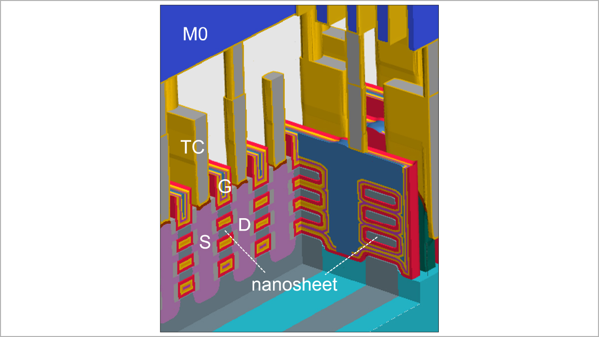
Gate-All-Around (GAA) transistors, also known as nanosheets or forksheets, represent a significant step beyond the FinFET architecture prevalent in modern high-performance chips. In FinFETs, the gate wraps around three sides of the channel. In GAA, the gate material completely encircles the channel on all four sides. This 360-degree gate control provides superior electrostatic integrity, drastically reducing short-channel effects like leakage current. For AI applications, this translates to transistors that can switch more reliably and with less wasted energy, enabling higher clock speeds and more operations per watt.
The primary advantage of GAA lies in its ability to maintain gate control even as transistor dimensions shrink. As transistors get smaller, the gate's ability to influence the channel can degrade, leading to performance inconsistencies and increased power leakage. GAA's conformal gate structure mitigates this by providing a more uniform and robust control mechanism. This enhanced control is particularly crucial for the high-density, high-performance requirements of AI accelerators, where millions or billions of transistors must operate in lockstep with maximum efficiency.
While GAA offers substantial benefits, its implementation presents manufacturing complexities. Fabricating nanosheets with precise dimensions and uniform gate coverage requires advanced lithography and etching techniques. The transition from FinFETs to GAA also necessitates changes in design automation tools and methodologies to account for the new device physics and layout considerations. Despite these challenges, leading foundries are already deploying GAA technology for their most advanced nodes, recognizing its necessity for future high-performance computing and AI chips.
Complementary FETs (CFET): The Next Frontier
Building upon the foundation of GAA, Complementary Field-Effect Transistors (CFET) represent the next logical step in transistor scaling. CFET integrates both NMOS (n-channel metal-oxide-semiconductor) and PMOS (p-channel metal-oxide-semiconductor) transistors in a vertical, stacked configuration. Instead of placing NMOS and PMOS transistors side-by-side, CFET stacks them one on top of the other. This vertical integration dramatically increases transistor density, allowing more transistors to be packed into the same area of silicon, or equivalently, enabling smaller chip footprints for the same functionality.
Think of CFET less like building more houses on a block, and more like building a multi-story apartment building on that same block. This vertical stacking is a critical innovation for AI hardware. AI models are becoming increasingly complex, requiring more transistors to execute. CFET allows designers to pack an unprecedented number of transistors into a given area, which is paramount for creating more powerful and compact AI accelerators, CPUs, and GPUs. The density gains are not just about shrinking; they are about enabling entirely new levels of computational capability within practical physical constraints.
The manufacturing complexity of CFET is even greater than that of GAA. Stacking different types of transistors with precise alignment and electrical isolation between them requires highly advanced fabrication processes. Furthermore, the design and routing of interconnects to these stacked devices become significantly more challenging. However, the potential benefits in terms of density and performance are so substantial that research and development efforts are heavily focused on overcoming these hurdles. CFET is seen as the path forward for continuing the scaling trajectory beyond the limits of current architectures, ensuring that the semiconductor industry can keep pace with the escalating demands of AI and other compute-intensive applications.
Enabling Technologies: Backside Power and DTCO
The full potential of advanced transistor architectures like GAA and CFET cannot be unlocked without complementary technological advancements. Two such critical areas are backside power delivery and Design Technology Co-Optimization (DTCO). As transistors shrink and become more densely packed, delivering power efficiently to every single device becomes a major bottleneck. Traditional frontside power delivery, where power and ground connections are routed on the same metal layer as the transistors, becomes increasingly congested and inefficient.
Backside power delivery, also known as backside power delivery network (BSPDN), moves the power and ground connections to the backside of the silicon wafer. This frees up valuable real estate on the frontside, allowing for more logic transistors and a cleaner routing environment. For AI chips, where power delivery is critical for sustained high performance and preventing voltage droop, BSPDN is becoming indispensable. It's like upgrading from a single-lane road to a multi-lane highway for electricity, ensuring that every computational unit gets the power it needs without traffic jams.
Design Technology Co-Optimization (DTCO) is the holistic approach that brings together chip designers and process engineers. It ensures that design rules and manufacturing processes are aligned to maximize the benefits of new transistor structures. For GAA and CFET, DTCO is essential for optimizing everything from the physical layout of the transistors to the choice of materials and the lithography techniques used. Without this close collaboration, designers might not be able to fully exploit the performance and density advantages offered by these new architectures, or manufacturing yields could suffer. The synergy between these enabling technologies and the new transistor designs is what will ultimately pave the way for the AI-powered future.