
Advancing Semiconductor Wafer Slicing with Femtosecond Lasers
The relentless demand for advanced semiconductor devices, particularly those requiring wide-bandgap materials like Silicon Carbide (SiC), necessitates innovative manufacturing techniques. Traditional wafer slicing methods, often involving mechanical sawing, can introduce significant material stress, subsurface damage, and kerf loss, impacting device performance and yield. In response, researchers from Texas A&M University, the Korea Institute of Machinery & Materials (KIMM), and the University of Science and Technology (UST) have published findings detailing a novel approach to slicing 4H-SiC wafers using femtosecond lasers. This method promises non-contact processing, reduced defects, and, crucially, precise depth control, overcoming long-standing challenges in laser-based material processing.
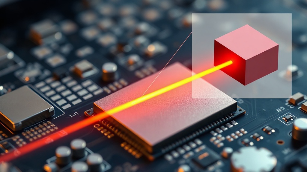
The core of this research lies in addressing the complex interaction between ultrashort laser pulses and materials exhibiting strong optical nonlinearities, such as 4H-SiC. When high-intensity ultrashort laser pulses enter such materials, phenomena like self-focusing and plasma generation can occur. These nonlinear effects obscure the direct relationship between the laser parameters and the resulting cut depth. Effectively, the laser beam's behavior inside the material becomes unpredictable, making it difficult to achieve consistent and controlled material removal. The team's breakthrough involves a sophisticated control mechanism that leverages these nonlinearities to achieve self-focusing control, thereby enabling depth-precise wafer slicing.
The Challenge of Laser-Material Interaction in SiC
Silicon Carbide, especially the 4H polytype, is highly sought after for power electronics due to its superior thermal conductivity, high breakdown electric field, and high saturated electron velocity compared to silicon. These properties enable devices that are smaller, more efficient, and capable of operating at higher temperatures and voltages, making them ideal for electric vehicles, renewable energy systems, and industrial applications. However, SiC is an extremely hard and brittle material, making it challenging to process with conventional methods. Traditional diamond-wire sawing, while effective, is slow, generates significant waste (kerf loss), and can induce subsurface damage that requires extensive post-processing and annealing steps. This adds cost and complexity to SiC device manufacturing.
Laser-based processing offers a compelling alternative. Femtosecond lasers, delivering energy in extremely short pulses (10⁻¹⁵ seconds), minimize heat diffusion into the surrounding material. This results in less thermal damage, reduced microcracking, and lower defect generation compared to longer-pulsed lasers. The process is non-contact, avoiding mechanical stress. However, achieving precise control over the depth of the cut is a significant hurdle. The intense electric fields of femtosecond laser pulses can induce nonlinear optical effects within the SiC. These effects include multiphoton absorption, avalanche ionization, and self-focusing, where the laser beam's intensity profile changes as it propagates through the material. This self-focusing can lead to unpredictable energy deposition, making it difficult to define a clean, straight cut at a specific depth. The researchers' paper, titled “Self-Focusing Control for Depth-Precise Wafer Slicing of 4H-SiC in Femtosecond Laser Processing,” directly tackles this complexity.
Self-Focusing Control for Precision Slicing
The research team's key innovation lies in their ability to harness and control the self-focusing phenomenon. Instead of viewing it as an obstacle, they have developed a method to utilize it for precise depth control. By carefully tuning laser parameters such as pulse energy, repetition rate, focusing conditions, and scanning strategy, they can predictably guide the laser's interaction zone within the SiC material. This is akin to steering a high-speed projectile not by directly controlling its path, but by subtly manipulating the medium it travels through to achieve a precise impact point. The self-focusing effect, when managed, can help concentrate the laser energy at the desired depth, enabling the creation of a precise cut or scribe line.
This controlled interaction allows for the slicing of SiC wafers into thinner layers with significantly reduced defects. The non-contact nature of the process eliminates mechanical stress, and the ultrashort pulse duration minimizes thermal damage. This leads to cleaner surfaces and edges, potentially reducing or even eliminating the need for subsequent grinding and polishing steps. The ability to control the depth precisely means manufacturers can slice wafers to exact specifications, optimizing material usage and enabling the production of thinner, more efficient SiC substrates for advanced power devices. The research demonstrates that this method can achieve high-quality cuts with minimal subsurface damage, a critical factor for high-performance electronic components.
Implications for the Semiconductor Industry
The successful implementation of this femtosecond laser slicing technique has profound implications for the semiconductor manufacturing industry, particularly for SiC devices. Firstly, it offers a pathway to higher yields. By reducing kerf loss and minimizing material defects, manufacturers can produce more functional devices per wafer, directly impacting cost-effectiveness. Secondly, it enables the production of thinner SiC wafers. Thinner wafers are lighter, easier to handle, and can lead to thinner, more compact power modules, which are crucial for applications like electric vehicles where space and weight are at a premium. Thirdly, the reduced need for post-processing steps simplifies the manufacturing flow, potentially shortening production cycles and lowering overall manufacturing costs.
Furthermore, this research contributes to the broader trend of adopting advanced laser processing techniques in semiconductor fabrication. As device geometries shrink and material requirements become more stringent, traditional manufacturing methods often reach their limits. Femtosecond lasers, with their precision and minimal impact, are becoming indispensable tools for tasks ranging from dicing and scribing to complex 3D structuring of semiconductor materials. The specific advancement in depth control for SiC slicing demonstrates that even challenging materials can be processed with high precision using these advanced laser technologies. The collaborative effort between academic institutions like Texas A&M, KIMM, and UST is vital in pushing the boundaries of material science and manufacturing technology, paving the way for the next generation of high-performance electronic devices.