Introduction: The Need for Custom Silicon
In the rapidly evolving landscape of networking, off-the-shelf Ethernet switch ASICs often fall short of meeting the specific performance, power, and feature requirements of cutting-edge applications. This is particularly true for hyperscalers, specialized research institutions, and companies developing novel network architectures. Designing a custom ASIC, while a monumental undertaking, offers unparalleled control and optimization opportunities. This article delves into the complex journey of designing an Ethernet switch ASIC, covering the key architectural decisions, design flows, and verification challenges involved.
Architectural Foundations: Defining the Core
The first critical step is defining the ASIC's architecture. This involves making fundamental choices about packet processing, buffering, and traffic management. Key considerations include:
- Packet Forwarding Engine (PFE): This is the heart of the switch. Decisions here revolve around the forwarding path (e.g., cut-through vs. store-and-forward), the complexity of the lookup engine (e.g., TCAM vs. SRAM for MAC tables, routing tables), and the support for advanced features like Access Control Lists (ACLs) and Quality of Service (QoS).
- Ingress/Egress Pipelines: How packets are processed upon entering and leaving the switch is crucial. This includes header parsing, modification, classification, and applying policies. The parallelism and pipelining of these stages directly impact throughput.
- Buffering Strategy: Managing buffer memory is essential for handling traffic bursts and preventing packet loss. This involves deciding on buffer sizes, memory architecture (e.g., shared vs. dedicated buffers), and buffer management algorithms (e.g., head-of-line blocking mitigation).
- Traffic Management: Implementing robust QoS mechanisms, shaping, policing, and scheduling algorithms ensures predictable performance for different traffic classes.
- Control Plane Integration: While the ASIC primarily handles the data plane, it needs interfaces and mechanisms to interact with the control plane (e.g., CPU, management interfaces) for configuration, statistics, and protocol handling.
The Design Flow: From Concept to Silicon
Designing an ASIC follows a rigorous, multi-stage flow:
1. Specification and High-Level Design
This phase translates functional requirements into detailed specifications. Architects define the macro-level blocks, their interfaces, and the overall system behavior. This is where the trade-offs between performance, power, area, and cost are first rigorously analyzed. Think of this stage like drawing the blueprints for a skyscraper: you define the number of floors, the layout of each floor, and the structural integrity required before any physical construction begins.
2. RTL Design and Synthesis
Engineers translate the architectural specifications into Register Transfer Level (RTL) code, typically using Verilog or VHDL. This code describes the hardware's behavior at a level of abstraction suitable for simulation and synthesis. The RTL code is then fed into synthesis tools, which convert it into a gate-level netlist – a description of the logic gates and their interconnections. This process requires careful timing constraints and optimization to meet performance targets.

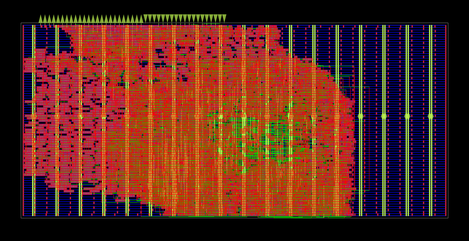
3. Physical Design
This is where the digital design is transformed into a physical layout that can be manufactured on silicon. It involves several sub-stages:
- Floorplanning: Arranging the major blocks on the chip die.
- Placement: Placing standard cells (basic logic gates) within the blocks.
- Clock Tree Synthesis (CTS): Distributing the clock signal to all sequential elements with minimal skew.
- Routing: Connecting the gates and blocks with metal wires.
- Timing Closure: Iteratively optimizing the layout to ensure all timing paths meet their deadlines.
- Physical Verification: Running Design Rule Checks (DRC) and Layout Versus Schematic (LVS) to ensure the design adheres to manufacturing rules and matches the schematic.
This stage is heavily reliant on Electronic Design Automation (EDA) tools and close collaboration with foundries for process technology information.
4. Verification and Validation
Verification is arguably the most challenging and time-consuming part of ASIC design. The goal is to ensure the design functions correctly under all possible conditions. This involves:
- Simulation: Running testbenches against the RTL code to check functional correctness. This can involve directed testing (specific scenarios) and constrained-random testing (generating vast numbers of random but valid inputs).
- Formal Verification: Using mathematical methods to prove or disprove specific properties of the design, catching corner cases that simulation might miss.
- Emulation and Prototyping: For complex designs, hardware emulation platforms or FPGAs are used to run the design at near-real-time speeds, allowing for more extensive testing, including early software development.
- Post-Silicon Validation: After the chip is fabricated, it is tested in a lab environment to confirm it meets specifications and to identify any manufacturing-related defects.
The complexity of modern ASICs means that verification can consume 60-70% of the total design effort.
Key Challenges and Considerations
Designing an Ethernet switch ASIC is fraught with challenges. Power consumption is a major constraint, especially for high-density, high-speed switches. Achieving low latency requires careful microarchitectural decisions and efficient pipeline design. Furthermore, the sheer complexity of the logic and the need for extensive verification demand highly skilled engineering teams and sophisticated EDA tools. The cost of non-recurring engineering (NRE) for a custom ASIC can be millions of dollars, making it a significant investment that must be justified by the benefits gained.
Conclusion: The Future of Network Customization
The design of an Ethernet switch ASIC is a testament to the intricate interplay of computer architecture, digital design, and verification methodologies. As network demands continue to escalate, the ability to tailor silicon to specific needs will become increasingly critical. While the path is arduous, the potential for performance gains, power efficiency, and unique feature sets makes custom ASIC design a compelling option for those pushing the boundaries of network technology.