The Evolving Landscape of High-Bandwidth Memory
High-Bandwidth Memory (HBM) is no longer a one-size-fits-all commodity. The explosive growth of artificial intelligence and high-performance computing workloads has created an urgent demand for memory solutions that are precisely tuned to specific application requirements. While standardized HBM offerings have served the market well, the era of custom HBM is dawning, promising greater performance, efficiency, and specialized capabilities. This shift is driven by the fundamental realization that generic memory architectures, while broadly capable, often leave performance on the table when confronted with the unique computational patterns of advanced AI models, complex simulations, and data-intensive analytics.
The need for customization stems from the diverse nature of these cutting-edge applications. AI training, for instance, might prioritize raw throughput and latency reduction for massive parallel computations. Inference, on the other hand, could benefit from lower power consumption and optimized memory access patterns for specific model architectures. Similarly, scientific simulations may require unique memory partitioning or specialized error correction capabilities. The current market, while robust, offers limited flexibility. However, the semiconductor industry is responding. Major foundries and memory manufacturers are increasingly exploring and offering tailored HBM solutions, moving beyond standard JEDEC specifications to meet the granular needs of leading technology companies.
The Drivers Behind Customization
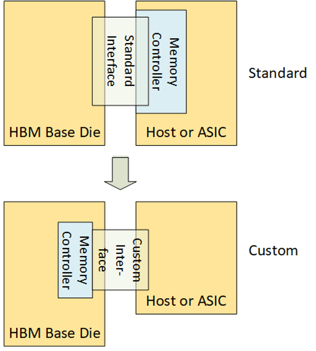
Several key factors are accelerating the move towards custom HBM. First and foremost is the insatiable appetite of AI. As AI models grow in complexity and scale, the memory subsystem becomes a critical bottleneck. Traditional DDR memory simply cannot keep pace with the data transfer rates required for training and deploying these models efficiently. HBM, with its stacked DRAM architecture and wide interface, offers a significant advantage. However, even within HBM, there are opportunities for optimization. Tailoring the memory controller, adjusting the number of memory stacks, or modifying the interface width can yield substantial performance gains for specific AI accelerators or GPUs.
Beyond AI, the increasing sophistication of HPC applications, advanced graphics processing, and emerging areas like autonomous driving also necessitate specialized memory. These fields often involve unique data structures, real-time processing demands, and stringent power budgets that a standardized HBM solution might not optimally address. For example, a company developing a next-generation autonomous vehicle system might require HBM with enhanced reliability features and deterministic performance under extreme environmental conditions, something not typically found in off-the-shelf products. This level of specialization is where custom HBM truly shines.
The competitive landscape is also a significant driver. Companies investing heavily in AI and advanced computing want every possible edge. Offering a custom HBM solution that provides a few percentage points of improved performance or a significant reduction in power consumption can translate into a substantial competitive advantage. This is particularly true for hyperscalers and large AI chip designers who have the scale and technical expertise to co-design these bespoke solutions with their silicon partners.
Business Models for Custom HBM
The emergence of custom HBM necessitates new business models and collaborative approaches. Unlike off-the-shelf components, custom solutions require deep engagement between the memory provider and the end-user. This often involves significant upfront investment from both parties, including co-design efforts, joint verification, and specialized manufacturing processes. The business model is shifting from a transactional sale of components to a more integrated partnership.
One potential model involves direct co-development and manufacturing agreements. In this scenario, a major AI chip designer might work directly with a memory manufacturer, such as SK Hynix or Samsung, to define the exact specifications of their HBM. This could include everything from the number of DRAM dies in a stack and the interface speed to specific thermal management features or embedded security elements. The memory manufacturer would then produce these custom HBM chips exclusively for that client. This approach offers the highest degree of customization but also requires the most significant commitment and carries the highest risk.
Another model could involve specialized design houses or IP providers who develop flexible HBM IP that can be licensed and integrated by various foundries or chip manufacturers. These entities would focus on creating modular HBM designs that can be easily configured to meet different customer needs, abstracting away some of the complexity of the underlying silicon. This approach democratizes access to custom HBM, allowing smaller players or those with less direct manufacturing access to benefit from tailored memory solutions.
A third model might see system-level integrators or platform providers offering customized HBM as part of a larger solution. For instance, a company building specialized AI server platforms could partner with memory vendors to offer pre-validated, optimized HBM configurations for their specific server architectures, simplifying the procurement and integration process for their end customers. This positions custom HBM as a value-added service within a broader product offering.
Challenges and Future Outlook
Despite the clear benefits, the path to widespread custom HBM adoption is not without its challenges. The primary hurdle is the sheer complexity and cost involved. Developing custom silicon, especially memory, requires immense engineering talent, advanced manufacturing capabilities, and substantial capital investment. The lead times for designing, verifying, and manufacturing custom HBM can also be lengthy, which may not align with the rapid iteration cycles common in the AI industry.
Another challenge lies in standardization versus customization. While custom solutions offer peak performance for specific tasks, a completely fragmented market with no common standards could lead to interoperability issues and hinder the broader ecosystem development. Finding the right balance between specialized, high-performance custom solutions and the need for some level of standardization will be critical for sustained growth. The industry will need to carefully define where customization adds the most value without fracturing the market entirely.
The surprising detail here is not that custom HBM is emerging, but the speed at which it is becoming a strategic imperative. What was once a niche consideration for bleeding-edge research is now a mainstream requirement for companies aiming to lead in AI and advanced computing. The future of HBM is undoubtedly custom, driven by the relentless pursuit of performance and efficiency in the most demanding computational environments. As AI continues its exponential trajectory, the ability to tailor memory to the workload will become a defining characteristic of next-generation computing platforms.
The Unanswered Question: Scalability of Customization
While the benefits of custom HBM are clear, what nobody has addressed yet is the long-term scalability of this custom business model. Can the semiconductor industry, with its already stretched supply chains and immense capital requirements, sustain a model where a significant portion of HBM production is dedicated to bespoke, low-volume, high-complexity designs? The transition from standardized products to highly differentiated custom solutions presents a significant operational and logistical challenge that will require innovative approaches to manufacturing, supply chain management, and potentially, a new generation of flexible fabrication technologies.