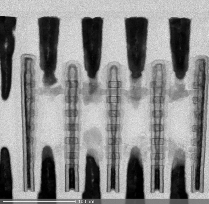
Pioneering CFET Integration Modules
The relentless pursuit of smaller, faster, and more power-efficient semiconductor devices has led the industry to explore advanced transistor architectures. Among these, Complementary Field-Effect Transistors (CFETs) represent a significant leap forward, promising to overcome the scaling limitations of traditional FinFETs and planar transistors. CFETs stack nFET and pFET devices vertically, enabling higher density and improved performance. However, realizing the full potential of CFETs requires overcoming substantial integration challenges. A recent advancement addresses two critical hurdles: the development of an improved backside contact module and a novel gate stack for threshold voltage tuning.
These innovations are crucial for moving the CFET-based device roadmap forward. The successful integration of these modules is not merely an incremental improvement; it's foundational to unlocking the performance gains promised by CFETs. Without robust backside contacts, signal integrity and power delivery become compromised. Similarly, precise control over threshold voltage (Vt) is paramount for managing power consumption and ensuring reliable operation across a wide range of applications, from high-performance computing to ultra-low-power IoT devices.
Improved Backside Contact Module
One of the primary challenges in CFET fabrication lies in efficiently routing signals and power to the stacked transistors. Traditional approaches often require complex lithography and etching steps, increasing manufacturing costs and potentially introducing defects. The newly developed backside contact module offers a more streamlined and effective solution. This module focuses on optimizing the fabrication process to ensure reliable electrical connection to the backside of the transistors, which is essential for the stacked nFET and pFET structures. By improving the contact resistance and reducing the parasitic capacitance associated with these connections, the new module directly contributes to higher device speed and lower power dissipation.
The significance of this improvement cannot be overstated. Think of it less like adding a new highway lane and more like redesigning the entire highway interchange to eliminate bottlenecks. A poorly designed backside contact is a choke point for both data and power. This novel module aims to smooth out that flow, enabling the stacked transistors to operate closer to their theoretical maximum performance. This is particularly important as feature sizes continue to shrink, making the physical space for contacts even more constrained. The ability to reliably access both nFET and pFET through a common or optimized backside infrastructure is key to dense CFET integration.
Novel Gate Stack for Threshold Voltage Tuning
Precise control over the threshold voltage (Vt) of transistors is fundamental to modern integrated circuit design. Vt determines the gate voltage at which a transistor begins to conduct current. In CFETs, where nFETs and pFETs are stacked, achieving independent and accurate Vt control for each device type within the same process flow is exceptionally difficult. Traditional methods often involve complex doping schemes or gate material variations that can be challenging to implement monolithically.
The novel gate stack configuration introduced in this work tackles this challenge head-on. It provides a mechanism for fine-tuning the Vt of individual transistors within the CFET structure without compromising the overall process flow or device integrity. This could involve new high-k dielectric materials, novel metal gate electrodes, or a combination thereof, engineered to interact differently with silicon channels for n-type and p-type conduction. The ability to precisely set Vt for both nFETs and pFETs allows designers to optimize the circuit for specific performance targets, such as maximizing speed for high-performance applications or minimizing leakage current for low-power scenarios. This level of control is essential for heterogeneous integration and for tailoring transistor behavior to the demands of diverse workloads.
Implications for the CFET Roadmap
These advancements in backside contact modules and gate stack configurations are not isolated technical achievements. They represent critical steps in validating and accelerating the broader CFET roadmap. By providing more robust and manufacturable solutions for key integration challenges, these innovations pave the way for the wider adoption of CFET technology in future generations of microprocessors, memory devices, and specialized accelerators.
The successful implementation of these modules suggests that the industry is moving beyond theoretical exploration and towards practical manufacturing solutions for CFETs. This progress is vital for maintaining the pace of Moore's Law and for enabling the development of increasingly complex and powerful electronic systems. The ability to achieve higher transistor density and better performance per watt is a direct consequence of overcoming such fundamental integration hurdles. The work highlights a concerted effort to mature CFET technology, moving it closer to high-volume manufacturing readiness.
Standard Cell Configurations and Future Directions
Beyond the fundamental device-level modules, the practical implementation of CFETs in complex integrated circuits requires the development of efficient standard cell libraries. These libraries contain basic logic gates (like NAND, NOR, and inverters) built using CFETs, optimized for area, power, and performance. The ongoing work in developing novel integration modules directly influences the design and capabilities of these standard cells. For instance, the improved backside contact and Vt tuning capabilities allow for denser, more power-efficient logic gates.
What remains to be fully explored is how these new CFET standard cell configurations will impact existing Electronic Design Automation (EDA) tools and methodologies. While the fundamental logic remains the same, the underlying transistor physics and layout rules for CFETs are significantly different. Ensuring that EDA tools can accurately model, place, and route these new cells without introducing unforeseen design complexities or performance degradations will be a critical next step. This transition requires close collaboration between semiconductor manufacturers, IP providers, and EDA vendors to ensure a smooth path from device innovation to functional silicon.
Ultimately, these advancements in integration modules and the subsequent development of optimized standard cell configurations are essential for realizing the full promise of CFET technology. They are enabling the next generation of semiconductor devices to push the boundaries of performance, power efficiency, and density, driving innovation across the entire technology landscape.