The Evolving Landscape of Chip Testing
The relentless march of artificial intelligence (AI) and high-performance computing (HPC) is pushing the boundaries of semiconductor design. These advanced System-on-Chips (SoCs) are becoming increasingly complex, featuring massive parallelism, intricate memory hierarchies, and specialized accelerators. While this innovation drives unprecedented computational power, it simultaneously creates significant challenges for the traditional methods used to test these chips before they reach consumers and enterprises. The sheer scale and complexity of modern AI/HPC SoCs mean that existing test strategies, which were adequate for simpler designs, are now hitting critical bottlenecks.
At the heart of the problem lies the immense volume of test data required to verify the functionality and performance of these sophisticated chips. Traditional testing involves generating vast patterns that exercise every logic gate and functional block. For devices designed for AI inference or HPC workloads, these patterns can be enormous, leading to prohibitively long test times and massive data storage requirements. Simply increasing the speed of test equipment or the capacity of storage is no longer a sustainable solution; it's akin to widening a single lane on a highway that's already gridlocked at every exit. The fundamental approach to testing needs to evolve to keep pace with the complexity of the chips themselves.
The industry has long relied on test compression techniques to mitigate the data volume issue. These methods aim to encode the large test patterns into smaller, more manageable streams. By reducing the amount of data that needs to be stored and transferred, compression can significantly decrease test time and associated costs. However, the excerpt from Semiconductor Engineering highlights a crucial point: compression, while valuable, only addresses half of the problem. Reducing the size of the test data is only effective if that data can be efficiently delivered to and processed by the chip under test. The bottleneck then shifts from data volume to data distribution and execution.
Beyond Compression: The Need for Efficient Data Distribution
The challenge of efficient data distribution is becoming increasingly prominent as SoC architectures grow more complex. Modern SoCs often feature multiple processing cores, dedicated AI accelerators (like NPUs or TPUs), high-bandwidth memory interfaces, and high-speed I/O. Testing these diverse functional blocks requires not only vast amounts of data but also the ability to deliver that data precisely when and where it's needed within the chip. Traditional Automatic Test Equipment (ATE) systems, while powerful, can struggle to keep up with the demands of these highly parallel and distributed architectures. The ATE must not only provide the compressed test data but also manage its decompression and application to the correct units under test (UUTs) without introducing new delays or limiting the test coverage.
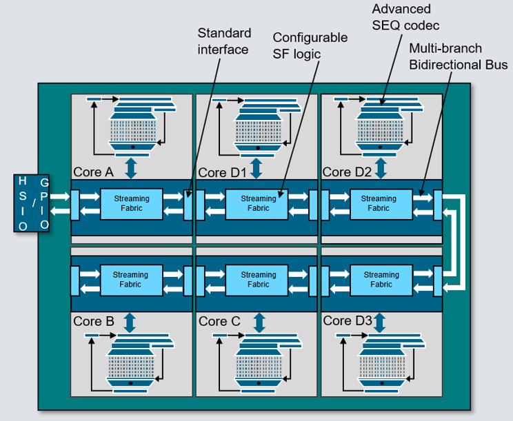
This is where the concept of hierarchical connectivity comes into play. Instead of a monolithic approach where a single ATE system manages all test operations, hierarchical testing breaks down the testing process into manageable levels. Think of it less like one giant orchestra conductor trying to direct every single musician simultaneously, and more like a conductor directing section leaders, who then guide their respective sections. In SoC testing, this means designating specific test controllers or embedded cores within the SoC itself to manage the testing of localized functional blocks or subsystems. The main ATE then communicates with these embedded controllers, providing high-level commands and overall test orchestration, while the embedded controllers handle the fine-grained test pattern delivery, execution, and result collection for their assigned domains.
This hierarchical approach offers several advantages. Firstly, it offloads some of the test execution burden from the ATE to the SoC itself, allowing the ATE to focus on tasks it does best, such as overall test program management and high-speed data acquisition. Secondly, it enables more efficient test pattern delivery. Instead of streaming potentially massive amounts of decompressed data across the entire SoC, the embedded controllers can access test data from local memory or even generate some test patterns on-the-fly. This significantly reduces the bandwidth requirements between the ATE and the UUT, and also minimizes the latency associated with data transfer across complex on-chip interconnects.
Hierarchical Connectivity in Practice
Implementing hierarchical connectivity requires careful consideration of the SoC's internal architecture. Design-for-Test (DFT) strategies must be adapted to incorporate test controllers and communication protocols that support this hierarchical model. This might involve leveraging existing on-chip interconnect fabrics, such as Network-on-Chip (NoC) technologies, to serve as the backbone for test data flow. Specialized test access ports (TAPs) or embedded test logic can be integrated to provide dedicated pathways for the ATE to communicate with the embedded test controllers. The choice of embedded controllers can vary; they might be dedicated test cores, or they could be repurposed existing processing cores or accelerators that are placed in a test mode.
The benefits of this approach are particularly pronounced for AI and HPC SoCs due to their inherent parallelism and distributed nature. For instance, an AI accelerator with hundreds or thousands of processing elements can be tested more effectively if a dedicated embedded controller manages the testing of clusters of these elements, rather than relying on a single ATE channel to probe each one individually. Similarly, complex memory subsystems, such as HBM stacks or large on-chip caches, can be tested more efficiently by local test logic that understands the memory's internal structure and can perform targeted tests without overwhelming the main test interface.
The integration of these advanced testing methodologies is not merely an incremental improvement; it represents a paradigm shift. As chip complexity continues to accelerate, driven by the insatiable demand for more powerful AI and HPC capabilities, the methods used to ensure their quality must evolve in lockstep. The future of SoC testing lies in a holistic approach that combines intelligent data compression with sophisticated, hierarchical distribution strategies, ensuring that the chips powering the next generation of technology can be both manufactured efficiently and verified thoroughly.
The surprise here is not that compression alone is insufficient, but the degree to which the industry is now looking inwards, leveraging the very complexity of the SoC itself to solve its testing challenges. It’s a subtle but significant shift in mindset, moving from external control to distributed, intelligent on-chip testing.